Return to CSCI 274 home page
Return to Dean Brock's home page
 Return to the UNCA Computer Science home
page
Return to the UNCA Computer Science home
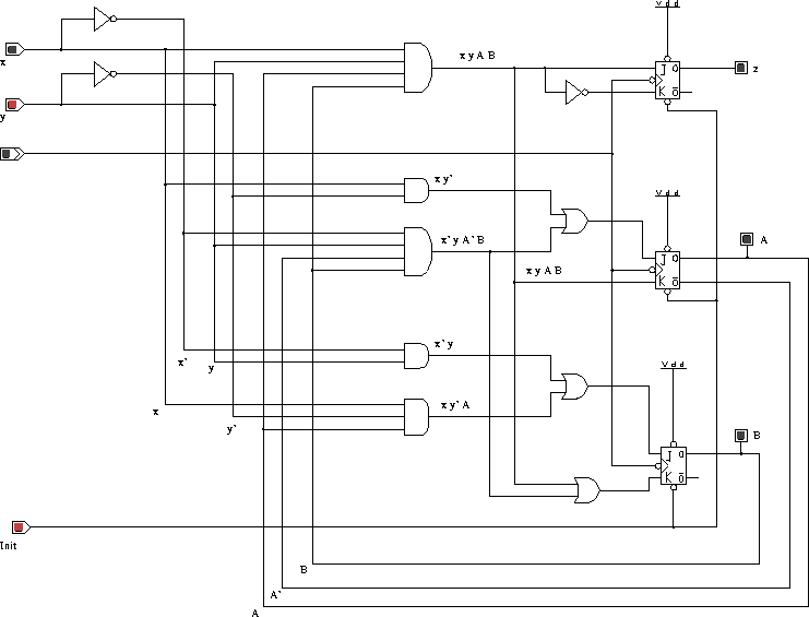
pageOnce again you will use your circuit from Lab 3 for this project. If you wish, you may work with your old teammates.
As usual
These commands will place two veriwell programs, combo1.v and combo2.v, into your directory.
The veriwell simulator will only run on a Sun SPARC workstation. If you are not logged into one of these machines type the following commands:
The veriwell program is very easy to run. All you need to do is type the command
Where circuit.v is a file that contains your veriwell program. The output of the simulation will be written to the file circuit.log.
The veriwell simulator compiles and executes programs written in Verilog HDL (Hardware Description Language), a very popular circuit specification language. Verilog HDL is a cross between C and RTL. C programmers will see may familiar constructs.
In CSCI 274, we will use the veriwell simulator of Wellspring Solutions on Verilog input. This program is actually a simplified version of Wellspring's commercial product, but it will work fine for the projects completed in the class.
If you have a PC at home that runs Windows 95, you can download a Windows version of veriwell from Wellspring's Veriwell 2.1 page.
First, look at the program combo1.v. This program starts with a dataflow specification of the combinatorial circuit used to solve the Nabs problem presented in class several weeks ago. The dataflow specification looks quite a bit like a C program, but all the statements are preceding by the keyword "assign".
The combinatorial circuit specification is followed by a stimulus module, a simple Verilog module that generates test cases for the combinatorial circuit.
After you have studied the program for a while, run the simulation by typing the command
Look at the output file combo1.log and see if it agrees with the truth table for the Nabs circuit after you have discarded the the dont-care output.
Now, look the Verilog program combo2.v. In this file the dataflow model of the combinatorial circuit has been replaced with a gate-level model that shows how the circuit can be built from inverters and NAND gates. Compare this specification with the diglog specified circuit.
Now use veriwell to test the gate-level model.
Create dataflow and gate-level models of your solution to the Lab 3 project. Call your dataflow model led-df.v and your gate-level model led-gl.v.
Return to CSCI 274 labs
Return to CSCI 274 home page
Return to Dean Brock's
home page
Return to the UNCA Computer Science home
page