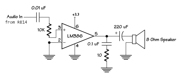
In this lab, we'll be working with sound again and to make that a more rewarding (and perhaps more deafening) experience we're going to use an amplifier. Your first task is to build the amplifier circuit shown below on your board.
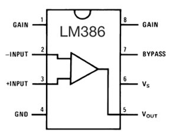
The triangular-shaped component in the schematic is an LM 386 Op Amp which is depicted below. The numbers in the schematic above are the component pin numbers shown below. The top of the LM386 is marked with a half-moon indentation identical to that marking the top of the PIC 24. There is also a semi-circular indent over pin 1 which enables you to determine the pin numbering.
Once you have built the amplifier circuit, test it using the music.mpc project that you developed in Lab 10.
| Demonstrate your new amplifier for your instructor. |
The PIC24 has built-in Analog-to-Digital Conversion (ADC), which, as the name implies, converts an analog input signal to a digital representation of that signal. Before we learn exactly how to program the PIC24 to work with analog input, let's learn more about the analog-to-digital conversion process.
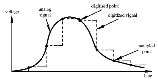
The real world is not digital. Consider temperature fluctuation as an example, it generally moves within some range of values without making large abrupt changes. We can measure aspects of our world like temperature, light intensity, forces, or whatever using analog sensors. In a digital device, the resulting signals are stored as sequential digital data. Consider the analog signal depicted below.
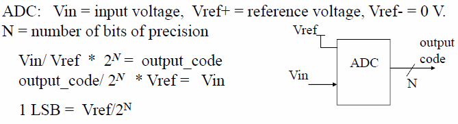
In a digital device, we discretize the input signal range (i.e., -VRef to 5 +VRef) into different voltage levels or intervals called states. The number of states is the resolution of the digital representation. Common resolution values range from 256 states (i.e., stored in 8 bits) to 4,294,967,296 states (i.e., stored in 32 bits). The PIC24 offers either 10 bits (the default) or 12 bits to store the state. Assuming the 10 bit default state representation with -VRef=0 and +VRef=3.3, the smallest voltage change that can be measured is (3.3-0)/210=3.3/1024 = 3.2mV. These calculations are expressed in your text as follows:
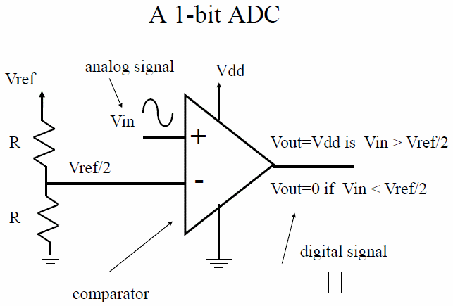
The translation of analog voltage values into different states is called Analog-to-Digital Conversion or ADC. For a one bit representation the process might be accomplished as follows:
A 10 bit representation can be created by extending this "flash" conversion process as depicted below.
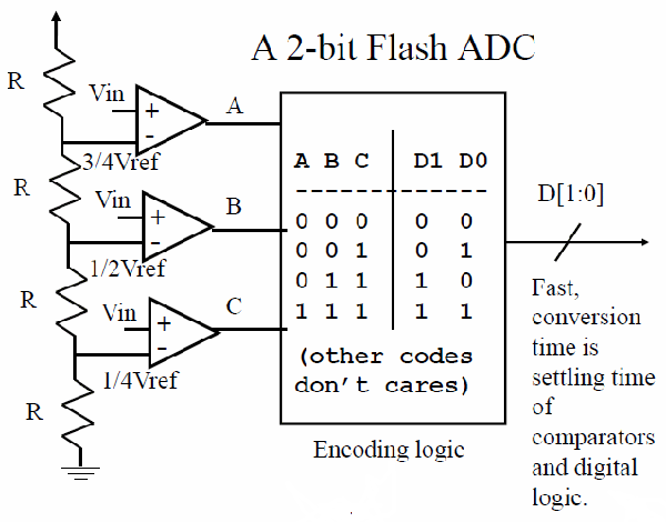
Of course such a conversion would be quick (1 clock cycle), but very costly from a hardware perspective (e.g., consider the number of comparators needed for 10 bits---2N-1 comparators). An alternative approach is that of "successive approximation."
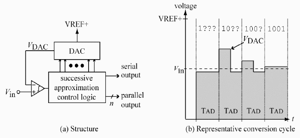
At the start of the successive approximation conversion, the input signal is placed in the hold mode, and the internal DAC Voltage (VDAC) is set to mid-scale(i.e., Vref/2). A comparator determines whether the input voltage is above or below the VDAC, and the result (bit 1, the most significant bit of the conversion) is stored in the successive approximation register. The VDAC is then set either to ¼ scale or ¾ scale (depending on the value of bit 1), and compared to the input signal to set bit 2 of the conversion. The result is stored in the register, and the process continues until all of the bits of the digital representation have been determined. The full conversion takes N (i.e., the number of bits set) clock cycles. Your text represents the process as follows, where TAD refers to clock cycles:
Although slower than "flash" ADC, "successive approximation" is less expensive and provides high precision. It is the ADC process of choice for many applications including the PIC24.
The built-in ADC features of the PIC24 are as follows:
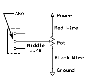
Now, let's use all of this good stuff. Begin by creating the analog input circuit depicted below on your breadboard.
Open chap11/adc_test.mcp from the the example code archive. Study the code, and then watch this silent video tutorial to better understand the program and its output. Compile and run adc_test.c and verify that the output is as expected.
| Show your instructor your program in action. |
As specified in Part 1 above, your speaker should still be connected to pin RB14 via the amplifier circuit. In the next program, you will use analog input on pin AN0 to control digital output on pin RB14. Begin by opening chap11/adc_test.mcp, if it is not already open. Create a new theremin.mcp project by saving the project with that name. Remove the file adc_test.c from the project and in its place add theremin.c. Open theremin.c and study the code. Compile and run the program. Use the pot to adjust the input voltage. Is the behavior what you expected?
| Show your instructor your new theremin program in action. |
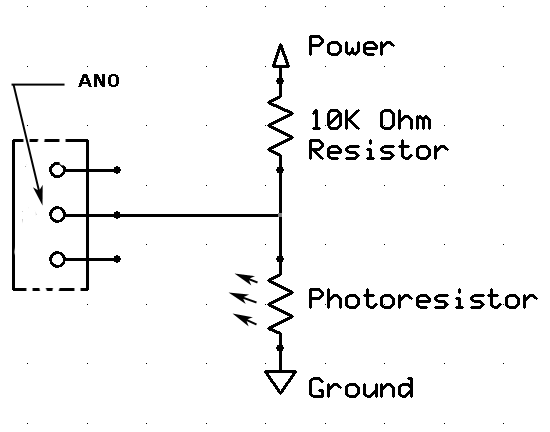
The tone produced by a theremin changes in response to the proximity of the hands of its player---that's not what we have right now. Create a better approximation to a theremin by replacing the potentiometer circuit with the one shown below. In the circuit below, you are using a photoresistor in a voltage divider and sensing the voltage between the two resistive elements. The resistance of a photoresistor changes in response to the light hitting its surface. The voltage at the midpoint of the voltage divider therefore changes as the light hitting the photoresistor changes.
Once you've created the theremin circuit, run theremin.mcp and play with your new instrument.
| Demonstrate your theremin for your instructor. |