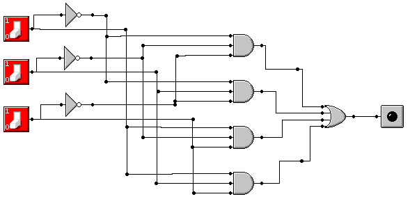
Draw a circuit that implements the truth table shown below. The "inputs" to the truth table are A, B, and C. The output is Z.
| input | output | ||
|---|---|---|---|
| A | B | C | Z |
| 0 | 0 | 0 | 1 |
| 0 | 0 | 1 | 0 |
| 0 | 1 | 0 | 1 |
| 0 | 1 | 1 | 0 |
| 1 | 0 | 0 | 0 |
| 1 | 0 | 1 | 1 |
| 1 | 1 | 0 | 0 |
| 1 | 1 | 1 | 1 |
A' B' C' +
A' B C' +
A B' C +
A B C
You'll notice that there is a minterm for every input combination where Z is 1. If you do not understand how to get this answer, you need to review section 3.3.4 and the Boolean synthesis spreadsheet shown in class. You'll need to do this problem "by hand" on the quiz. By the way, A' C' + A C is a more efficient solution, but that's a topic for CSCI 311.
Assume x is a C integer variable. Describe how you would set bits 1, 4, and 7 of x to 1 and clear bits 2, 5, and 13 to 0. You can do this in one statement.
x = (x | 0x92) & ~0x2024 ;
The binary number with bits 1, 4, and 7 set to 1 is 000010010010, which is hexadecimal 0x92. OR'ing this pattern into x will set the appropriate bits. Clearing bits is a bit more tricky. You need to AND with a pattern holding 0 where you want to clear and 1 elsewhere. Since the binary number with bits 2, 5, and 13 set to 1 is 0010000000100100, or hexadecimal 0x2024; you need to AND with ~0x2024. If you want more practice, you can try out a masking spreadsheet.
Implement the following Boolean function using only NAND gates and inverters:
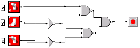
If you have an AND-OR solution, just replace the AND's and OR's with NAND's.