 button.
This will cause the shadow of an AND gate to follow your cursor
around. Click once within the main schematic window to place an AND
gate.
button.
This will cause the shadow of an AND gate to follow your cursor
around. Click once within the main schematic window to place an AND
gate.(The material in this lab was taken in part from a laboratory exercise developed for CS61c: Great Ideas in Computer Architecture, a course offered at UC Berkely.)
Launch Logisim by opening a terminal window under Linux and entering the command:
You can learn about Logisim beyond the scope of this lab (or download it to use at home) from the Logisim website.
We'll begin by creating a very simple circuit just to get the feel for placing gates and wires.
1. Start by opening the "Gates folder" in the "Explorer window" at the left of the screen. Click the "AND gate"
button.
This will cause the shadow of an AND gate to follow your cursor
around. Click once within the main schematic window to place an AND
gate.
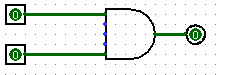
2. Click the "Input Pin"  button on the menu bar. Now, place two input pins somewhere to the left of your AND gate.
3. Click the "Output Pin"  button on the menu bar. Then place an output pin somewhere to the right of your AND
gate. Your schematic should look something like this at this point:
button on the menu bar. Then place an output pin somewhere to the right of your AND
gate. Your schematic should look something like this at this point:

4. Click the "Select and Add Wires" ![]() tool on the menu bar.
Click and drag to connect the input pins to the left side of the AND
gate. This will take several steps, as you can only draw vertical and
horizontal wires. Just draw a wire horizontally, release the mouse
button, then click and drag down starting from the end of the wire to
continue vertically. You can attach the wire to any pin on the AND gate
on the left side. Repeat the same procedure to connect the output (right
side) of the And Gate to the output pin. After completing these steps your
schematic should look roughly like this:
tool on the menu bar.
Click and drag to connect the input pins to the left side of the AND
gate. This will take several steps, as you can only draw vertical and
horizontal wires. Just draw a wire horizontally, release the mouse
button, then click and drag down starting from the end of the wire to
continue vertically. You can attach the wire to any pin on the AND gate
on the left side. Repeat the same procedure to connect the output (right
side) of the And Gate to the output pin. After completing these steps your
schematic should look roughly like this:
5. Now remove the unused inputs on the AND gate. Click on the gate and set "Number of Inputs" to 2 in the gate's "Attributes Table" located below the "Explorer window."
6. Finally, click the "Poke"  tool and try clicking on the input pins in your schematic. Observe what
happens. Does this match with what you think an AND Gate should do?
tool and try clicking on the input pins in your schematic. Observe what
happens. Does this match with what you think an AND Gate should do?
A schematic can contain subcircuits. In this part of the lab, we will create a subcircuit and demonstrate its use.
1. Create a new schematic (File->New) for your work.
2. Create a new subcircuit (Project->Add Circuit ). You will be prompted for a name for the subcircuit; call it MyNAND.
3. In the new schematic window that you see create a simple NAND circuit with 2 input pins on the left side and an output pin on the right side.
4. Go back to your "main" schematic by double-clicking "main" in the circuit selector at the left of the screen. Your original (blank) schematic will now be displayed, but your MyNAND circuit has been stored.
5. Now, single click the word "MyNAND" in the list. This will tell Logisim that you wish to add your "MyNAND" circuit into your "main" circuit.
6. Try placing your MyNAND circuit into the "main" schematic. If you did it correctly, you should see a box with 2 input points on the left and one output point on the right. Try hooking input pins and output pins up to these and see if it works as you expect.
7. Now use your MyNAND subcircuit to create an AND circuit. Do not use any of the built-in gates to create your AND circuit.
Hint: You were shown how to implement an AND gate using 2 NAND gates in lecture.
| Show your AND circuit constructed from MyNANDs to your instructor. |
Between lecture, your reading, and this lab, you now have all the tools needed to take a truth table and implement it in a Logisim schematic. Given the following truth table, complete the tasks below.
| c | b | a | | | x |
|---|---|---|---|---|
0 |
0 |
0 |
| |
0 |
0 |
0 |
1 |
| |
1 |
0 |
1 |
0 |
| |
1 |
0 |
1 |
1 |
| |
1 |
1 |
0 |
0 |
| |
0 |
1 |
0 |
1 |
| |
0 |
1 |
1 |
0 |
| |
0 |
1 |
1 |
1 |
| |
1 |
1. From the truth table above derive the Canonical SOP boolean equations for x.
2. Implement your boolean equations in your "main"
schematic in Logisim using standard gates. Be sure you label your input and
output pins using either the "Label" field of the pin (located in the "Attributes Table" below the "Explorer window") or the "Text"  tool. To use the text tool, select the tool and click on your schematic
and start typing. If you make a mistake, you can edit the text by
selecting your text object using the "selection"
tool. To use the text tool, select the tool and click on your schematic
and start typing. If you make a mistake, you can edit the text by
selecting your text object using the "selection"  tool, and edit the "Text" property in the property list below the "Explorer window" at the left of the screen.
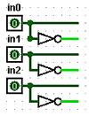
3. Your circuit will (potentially) require 3 inputs and the negation of each of those inputs. The figure below represents three inputs and their negations in an easy-to-read ( standard) layout. Use a similar layout in your circuit.
| Show your canonical SOP of the truth table to your instructor. | |
| Show your working schematic to your instructor. |
Although the circuit that you designed above may be correct---it may implement the truth table---it may not be the most efficient implementation of that table. Very often it is possible to simplify the logical expression representing a truth table using boolean algebra rules. The procedure for doing this can be automated and represented graphically, typically as a Karnaugh Map. Logisim implements such a simplification procedure and you can use that implementation to identify the most efficient circuit representing a truth table.
1. Select "main" in the "Explorer window" and verify that the circuit representing the truth table is showing in Logisim's circuit window. If not, select the project that contains the truth table circuit.
2. Select "Project" from the menu bar and then select "Analyze Circuit" from the drop-down menu.
3. In the Combinational Analysis window that appears, select the "Minimized" Tab, set the minimized logic expression as the working expression using the "Set As Expression" button and select the "Build Circuit" button to see the new (simpler) implementation of the truth table.
4. Investigate the other tabs on the Combinational Analysis Window.
| Show your simplified schematic to your instructor. |