This lab will be worked using Logisim. Start Logisim by opening a terminal window under Linux and entering the command:
In last week's lab we built a sequential logic component called a flip-flop, and we observed that this component can store its state. It is a primitive memory element; 8 flip-flops can be used to form one 8-bit register. In this lab, we will delve further into sequential logic circuits by constructing a Finite State Machine (FSM) that uses flip-flops to store its state. It is a bit too ambitious to breadboard even a simple FSM in a little over one hour, so we'll build our FSM in Logisim. You can re-acquaint yourself with Logisim by looking at Lab 1.
A finite state machine is not a "real" machine. It is a mathematical abstraction of a machine that could be built from combinatorial and sequential logic components. Our focus is on building the machine using logic components, not on designing the finite state machine. None-the-less, it's important to have a clear picture of the entire process because it is very powerful. So we'll look at the process of creating a finite state machine as well as building one using How To Design A Finite State Machine developed at Princeton University. Read that tutorial and answer the questions below before proceeding.
Questions
| Verify your answers to the questions above with your instructor, if you are uncertain of the correct answer. |
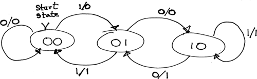
You're going to build the FSM specified in the finite state diagram below. This a slightly more complicated diagram than the one presented in the tutorial. This FSM has one input (to the left of the slash on the state transitions), one output (to the right of the slash on the state transitions), and three states.
This finite state machine outputs the result of integer division by 3. The input is the dividend in binary, the states represent the current remainder, and the output is the quotient in binary. The FSM accepts the binary dividend one bit at a time, most significant bit first, and generates the binary quotient one bit at a time, again, most significant bit first.
The states represent the current remainder in the division, in fact, the same FSM diagram with different outputs can be used as a modulo 3 calculator. If the value of the number entered so far is N, then after the digit b is entered, the value of the new number N' is 2N + b. Using this fact:
This leads to the following state transition diagram where the states are labeled with the value of (N mod 3) in binary.
Given the state transition diagram above, your first job is to fill in the state transition truth table below. Note:
| CS1 | CS0 | Input | NS1 | NS0 | Output |
|---|---|---|---|---|---|
| Show your truth table to your instructor. |
There are two steps remaining to complete your FSM:
This section focuses on the first step. For each subcircuits, you should write a Boolean expression that states its output as a function of its inputs; these are combinatorial circuits. You should derive these boolean expressions from the truth table formulated in Part 2. Use the Sum of Products (SOP) method used in Lab 1. The SOP method (although it is not called that) is also illustrated in the FSM tutorial, provided as part of this lab. You do not need to simplify these expressions.
| Show your Boolean expressions to your instructor. |
We will build the FSM in three parts: (1) the next-state subcircuit, (2) the output subcircuit, and (3) the flip-flops that will store the "state" of the FSM.
Although you are not required to do so, it is recommended that you implement the two combinatorial logic subcircuits (the next-state logic and the output logic) using the features provided in the "Combinational Analysis" window. Specifically, you can enter either the boolean expressions or the truth table that define each of these subcircuits in the "Combinational Analysis" window, and, using that information, Logisim will build the subcircuit for you.
Note: Be sure to enter the input and output variable names before entering either the boolean expressions or the truth table for each combinational logic subcircuit.
| Show your next-state and output subcircuits, implemented in Logisim, to your instructor. |
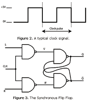
We will use synchronous D flip-flops to store the state of the FSM. Please read the short information panel on synchronous D flip-flops before proceeding.
Synchronous means that the flip-flop is concerned with time. Digital circuits can have a concept of time by using a clock signal. The clock signal simply goes from low-to-high and high-to-low in a short period of time.
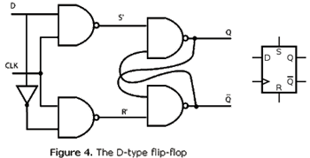
A D flip-flop is a slight variation of the synchronous flip-flop shown above. The figure below shows a sketch of the D flip-flop we will be using. This is a positive edge triggered D flip flop. In addition to the clock input, it has a data input D. It holds a single bit of state, which is visible on its output Q. On the rising edge of the clock it captures D and stores it internally. The schematic symbol for the D flip-flop is also shown below.
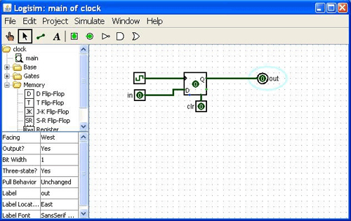
In Logisim, start a new project. Open the Memory folder in the Explorer window and you will see a D Flip-Flop. Add one to your empty schematic. Mouse over its pins so you can see its connections. You can read about it under Help. Connect an input pin to D and an output pin to Q. In the Base folder you will find a special pin called Clock. Drop it in and connect the flip-flop to the clock. It should look something like the image below.
Poke at D and see that nothing changes. You can poke clock, but Logisim has special support for the clock. Pull down the Simulate menu and select "Logging..." Begin by selecting the components that you want to monitor. Move to the "Table" tab under the Simulate menu and select "Reset Simulation." Now, set the tick frequency to 4 Hz and select "Ticks Enabled," both located on the Simulate menu. Make sure that you understand the output displayed under the Table tab. Note: You still need to "poke" the input to D to change it's value.
Now that you understand how to work with flip-flops in Logisim, build your complete FSM by linking the next-state and output subcircuits to your D flip-flops. Be sure to test your FSM using "logging" as described above.
| Show your FSM and logging window to your instructor. |