
(The material in this lab was taken largely from a laborator exercise developed by W. J. Dally for "CS 99S: The Coming Revolution in Computer Architecture: What To Do With One Billion Transistors," a course offered at Stanford University in 2001.)
You will need the following equipment/components to create the circuits in today's lab:
We can perform a logical function by connecting two switches – or two transistors together in series or parallel. In the examples below, we are using 2 NPN transistors to connect the output to ground, or "pass 0;" the inputs are applied to the bases of the transistors. The terminal c at the left below will be connected to 0 if inputs a AND b are both 1. Similarly, terminal f at the right below will be connected to 0 if either d OR e (or both of them) is 1.
We can build similar series and parallel circuits out of PNP transistors. Also, while these are 2-input series and parallel networks, we can extend these circuits to handle an arbitrary number of inputs.
To be "composable" a circuit must generate an output that is suitable for use as an input to a similar circuit. A simple series or parallel combination of NPNs as shown above won't do this because the input needs to be either 0 or 1, and the emitter of a NPN should be tied to ground. We need to add PNPs (or a resistor) to generate a 1 on the output in this state.
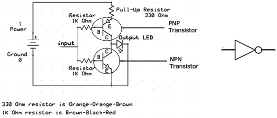
The simplest composable circuit is the inverter, shown above along with its schematic symbol. When the input is a 1, the NPN is on and the PNP is off, so the output is 0. Similarly, when the input is 0, the output is connected to 1 via the PNP and the NPN is off. To save time in drawing, we use the schematic symbol on the left to indicate an inverter and omit the power supply connections (to 1 and 0). In short, the inverter generates the logical inverse of its input.
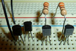
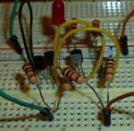
Create the inverter described in the schematic above. The input is provided manually by connecting the input wire to either power or ground. Be sure to test your inverter before showing it to your instructor.
| Show your inverter circuit to your instructor. |
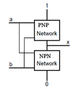
To implement a logical function of multiple signals, we build a logic gate, as shown below, by replacing the PNP of the inverter with a network of PNPs that pulls up (connects the output to 1) when some logical function, f, of the inputs is true, so the output, x, is 1 when f(a, b, …) is true. To handle the case when f is false, we replace the NPN of the inverter with a network of NPNs that pulls down the output (connects it to 0) when f is false, so the output x is 0 when ~f(a,b,…) is true.
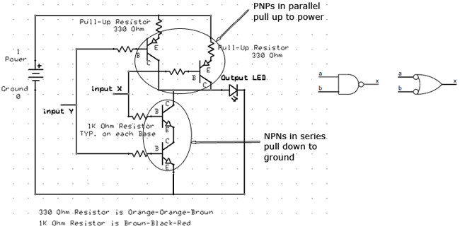
We make a NAND gate (or not-and) gate, as shown below, by using a series network of NPNs for the pull-down side of the gate – so the output is 0 when a AND b are both 1. We use a parallel network of PNPs to pull up the output when a OR b is zero. The circuit diagram for the NAND and its schematic symbols are shown below. The schematic symbol on the left reflects the x = ~(a ∧b) interpretation – the squared-bottom gate symbol means AND and the bubble (as above) means NOT, so x = NOT(a AND b) or ~(a ∧b). The symbol on the right is the x = ~a∨~b interpretation, the rounded-bottom gate symbol means OR and the inversion bubbles again mean not, so x = (NOT a) OR (NOT b) or ~a∨~b. This is the same function as ~(a ∧b) – write out the truth tables to convince yourself if you're not sure.
This approach to implementing logic functions using a network of PNPs to pull the output up and a network of NPNs to pull it down is only sufficient for "inverting" logic functions. This is because the NPNs take a 1 input to generate a 0 output and the PNPs take a 0 input to make a 1 output. To build non-inverting logic gates such as an AND gate, we need to use multiple levels. For example, to build an AND gate, the first level could be a NAND gate and the second level an inverter.
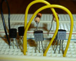
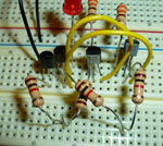
Your job is to create the NAND gate described in the schematic above. Because this is a somewhat complicated circuit, you are encouraged to follow the procedure below.
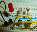

| Demonstrate the functionality of your NAND gate for your instructor. |
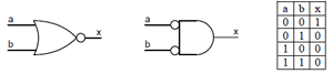
Another useful gate is the NOR gate which has the equation x = ~(a∨b). The two symbols for the NOR gate are shown below along with the truth table for a NOR.
On paper, draw the schematic for a NOR gate constructed from PNP and NPN transistors.
| Show your schematic for a NOR gate to your instructor. |