This lab uses a small combinational circuit to illustrate certain aspect of SystemVerilog using software available from Altera. If you would like a more detailed example using finite state machines, try out Altera’s Using ModelSim to Simulate Logic Circuits in Verilog Designs. Try download the example programs first.
You can also find a pretty good overview of Verilog in the Verilog overview & references page at Texas A&M.
Starting modelsim
Go to the command line and execute the following commands to create a directory for your 320 SystemVerlog programs.
mkdir -p ~/csci/320/svlabs
To start up ModelSim type the following command.
/opt/altera_lite/15.1/modelsim_ase/bin/vsim &
If you would like to save some typing in the future, you can either lock vsim to your launcher or type the following command to create a link to the executable.
ln -s /opt/altera_lite/15.1/modelsim_ase/bin/vsim ~/bin
If you had run a previous version of vsim and would like to clean up your environment, delete the .modelsim file in your home directory.
rm ~/.modelsim
Creating a ModelSim project
In the ModelSim program, use the menu choices
File ⇒
New ⇒
Project.
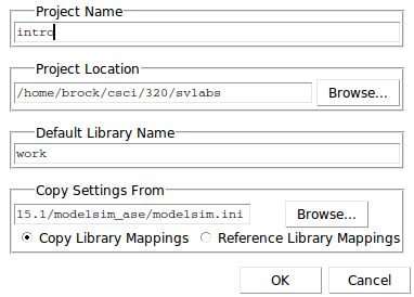
Next use
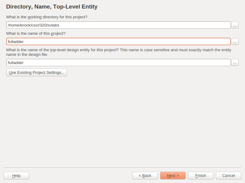
/home/username/csci/320/svlabs,
where username is your login name,
as the Project Location
(it would be safer to use the Browse
button to make the selection)
and use
intro as the
Project Name.
Next, you’ll see a little window.
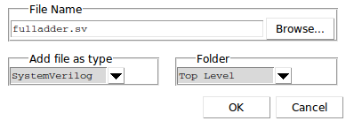
Press Create New File.
Create a file with the name
fulladder.sv
and the type of SystemVerilog
Make sure you use the type SystemVerilog and not the default VHDL.
You can now close the dialog box for adding more items to the project.
Go back go the command line, type the following command to make sure you have files in the right place. You should see five files in two different directories.
ls -lR ~/csci/320/svlabs
Completing the SystemVerilog program
Under the Project tab, double-click on fulladder.sv . This will allow you to start editing your program
You won’t get much help from ModelSim in getting started, so insert the following as your SystemVerilog program.
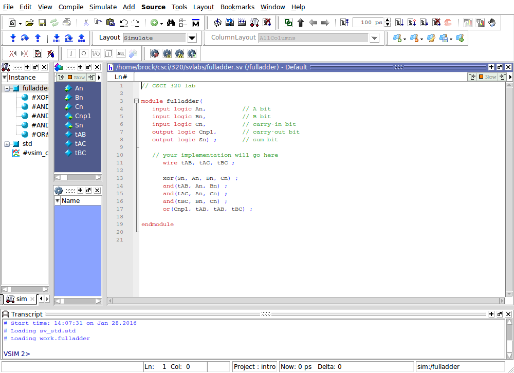
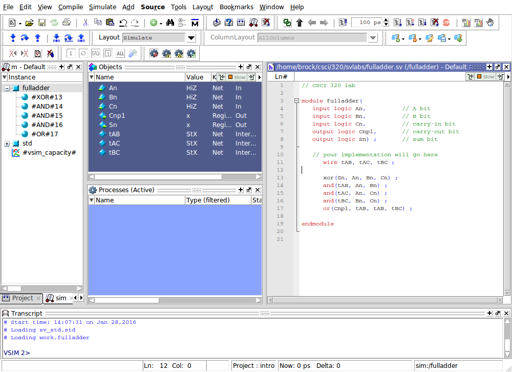
// CSCI 320 lab

module fulladder(
   input logic An,          // A bit
   input logic Bn,          // B bit
   input logic Cn,          // carry-in bit
   output logic Cnp1,       // carry-out bit
   output logic Sn) ;       // sum bit

   // your implementation will go here

endmodule
All the modifications you do to this program will be made
between the module header
and the endmodule keyword.
Notice that SystemVerilog doesn’t use C/Java-stylebraces
The keywords module
and endmodule surround the “function.”
SystemVerilog is a bit old fashioned.
In this lab are going to implement a full-adder circuit. You can find a detailed description of the full-adder circuit in Circuits Today. You can also find an interesting picture of one on Discovery magazine.
A structural implementation
In SystemVerilog declare three wires for connecting your gates.
After the comment about where your implementation will go,
add a declaration for three wires, which will be of type
logic.
(In Verilog, they would be of type wire.)
logic tAB, tAC, tBC ;
Now implement your module by placing the
the following structural description after the logic
declaration.
All your inputs, outputs and wires are now used in your program.
      xor(Sn, An, Bn, Cn) ;
      and(tAB, An, Bn) ;
      and(tAC, An, Cn) ;
      and(tBC, Bn, Cn) ;
      or(Cnp1, tAB, tAB, tBC) ;
The and, or and xor are some
of the predefined gates that are provided by SystemVerilog.
If you want to name your gates, you can use the following syntax.
(It’s an either-or. You can’t have both the named and
unnamed versions.)
      xor  sum(Sn, An, Bn, Cn) ;
      and  abTerm(tAB, An, Bn) ;
      and  acTerm(tAC, An, Cn) ;
      and  bdTerm(tBC, Bn, Cn) ;
      or   carry(Cnp1, tAB, tAC, tBC) ;
Be sure you have saved your code with Save. (NetBeans seems to do a much better job of saving than ModelSim.) Go ahead and compile your module with Compile ⇒ Compile All. The result of the compile will appear in the Transcript window. If there are errors, you will need to use View ⇒ Message View window to uncover the messages.
Go back to the command line, and repeat your ls command. Take another look at your files. fulladder.sv should be about 450 characters long.
Command-based simulation of the full adder
Getting ready to simulate
Press
Simulate ⇒
Start Simulation.
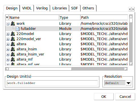
This will raise the
Start Simulation window,
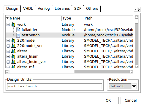
where you must expand the work library to
select the fulladder module.
For some reason, I had to restart the program on the newest version. to get this to work. Others had to use Project ⇒ Update. Also, explicitly saving your file might solve the problem. NetBeans seems to do a better job at this.
If all works well, there should be a flurry of flashing windows.
Use your mouse to reframe some of the windows.
Take a minute to look at these windows.
The Transcript window
is the console for a TCL
program that controls the simulation.
In the real world, designers write TCL scripts to
customize the simulation.
In the Objects window,
notice the values of your variables.
For now, consider HiZ and StX
to be uninitialized values.
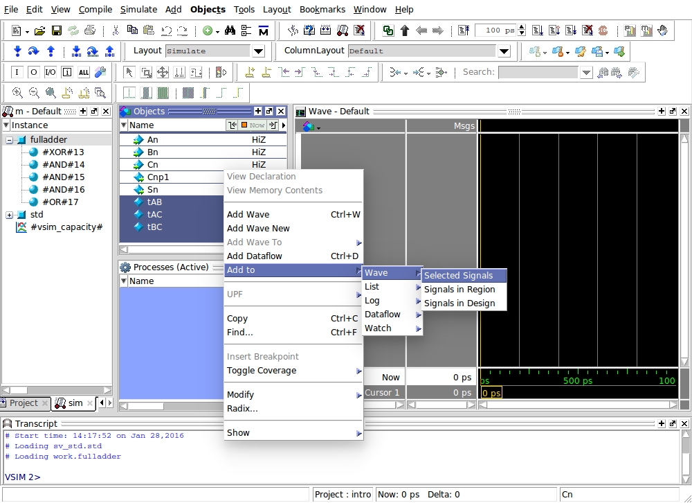
We want to put the input and output ports on the wave.
Use View
⇒ Wave to dispay the wave and add the
select the input and output signals to the wave.
Running the full adder
In the Transcript window, issue the following commands.
force An 0
force Bn 0
force Cn 0
run 100
This will initialize An, Bn and
Cn and
“run” your
circuit for 100 picoseconds.
You should see that all your variables now have the value
St0, a strong 0.
Now set An to 1 and run for another 100.
The values of An and Sn should change.
All those buttons
It is possible to use all those buttons to simulate your program. You can run your mouse slowly over the buttons or you can read the Altera tutorial or you can just keep typing commands.
Riding the wave
You can always mash
Simulate ⇒
Run ⇒
Restart to
reinitialize the simulation,
but then you will then to force all your variables.
Set An back to 0 and run another 100.
You should now see your values displayed on the wave.
Let’s to go through all eight combinations of the input using a Gray code. Use these 16 commands to do the checking. Each time you type run 100, make sure the outputs look correct.
force Cn 1
run 100
force Bn 1
run 100
force Cn 0
run 100
force An 1
run 100
force Cn 1
run 100
force Bn 0
run 100
force Cn 0
run 100
force An 0
run 100
Kind of tedious, ain’t it? Go ahead and stop the simulation with Simulate ⇒ End Simulation, and we’ll try something better.
A testbench program
Let’s add a testbench module to the project The testbench module will not be synthesized. It is purely for debugging.
You’ll need to create a new file. Select the Project tab and follow that with Project ⇒ Add to Project ⇒ New File. Name the new file testbench.sv and make sure it is of type SystemVerilog. It will not be added to the library until it is successfully compiled.
In this section of the lab, you will modify only the testbench module.
Do not modify the fulladder module.
SystemVerilog without a circuit
Here is the code for the testbench module.
This looks a lot like a C or Java loop to print
from 0 to 7,
except that it uses begin-end rather
than curly braces to surround the body of the for.
module testbench() ;
   logic[2:0]  vin ;
   integer i ;

   initial begin
      for (i=0; i<8; i=i+1)
      begin
         vin = i ; #100 ;
         $display("vin = %h", vin) ;
      end
   end
endmodule
The #100 is SystemVerilog’s way of delaying for
100 picoseconds.
Compile all your programs.
Start the simulator but choose only
testbench for the simulation.
(Be sure the testbench has been added to the project.
I had trouble seeing testbench and had to
close fulladder and then click on the testbench
and compile it. Odd.)
Either press the Run -All button (if you can find it) or just type run -all to start the simulation. (About the only thing the buttons do is talk to TCL.)
You should get a count from 0 to 7.
Go ahead and end the simulation and we’ll try for something a bit more useful.
Testing the full adder
Now we are going to add a “call”
of the fulladder module from the testbench.
To do this, you need a wire to connect
the output of
fulladder to the testbench.
The fulladder will be instantiated as
dut, for device under test.
This is a common naming convention in Verilog.
Place the following two
statements right before the initial begin keywords
to instantiate the fulladder and connect it to the testbench.
  logic[1:0] vout ;

  fulladder dut(vin[2], vin[1], vin[0], vout[1], vout[0]) ;
Next go into the initial begin block
and modify the call to $display so that
in prints out vout.
We are using the %b format specifier to print the
number in binary.
$display("vin = %b, vout = %b", vin, vout) ;
Compile all your programs but save them first. Start up the simulation, but select only the testbench. It will include the needed copy of the device under test. Hopefully, you will get the right answers.
Back on the wave
Try out the wave simulator by adding in
vin and vout.
You will need to expand them to see the individual bits.
Testbench is complete
At this point, your work on the testbench is complete.
You should never modify the testbench module again.
A behavioral description
The structural description is a good way to match a circuit, but it doesn’t look like a program.
Go to the fulladder and comment out
the structural description. Just enclose everything from the
wire declaration to the or gate with
the usual Java/C /* and */ comment delimiters.
Now add in a simple behavioral description.
      assign Sn = An ^ Bn ^ Cn ;
      assign Cnp1 = An & Bn | An & Cn | Bn & Cn ;
Except for the assign keyword, it looks just like
C or Java. Simulate it to see that it works fine.
If you don’t like those logical C/Java operators, you can just
use the regular addition operator, but you need to add a
two-bit declaration of a variable sum2bit to do this.
     logic[1:0] sum2bit ;

     assign sum2bit = An + Bn + Cn ;
     assign Sn = sum2bit[0] ;
     assign Cnp1 = sum2bit[1] ;
Again, simulate.
Finally, you can also take advantage of Verilog’s own special use of braces to concatenate bitstrings to write a one-statement implementation.
assign {Cnp1, Sn} = An + Bn + Cn ;
And simulate one more time.
Trying out Quartus
Exit from ModelSim and start up Quartus. (It may take a while for Quartus to start.)
/opt/altera_lite/15.1/quartus/bin/quartus &Use the menu choices File ⇒ New Project Wizard to create a Quartus project for synthesis. The project wizard will guide you through many screens. In one of the early screens, create your project in the same directory that you used above. and select
fulladder as your top-level design entry.
Also, go with an empty project.
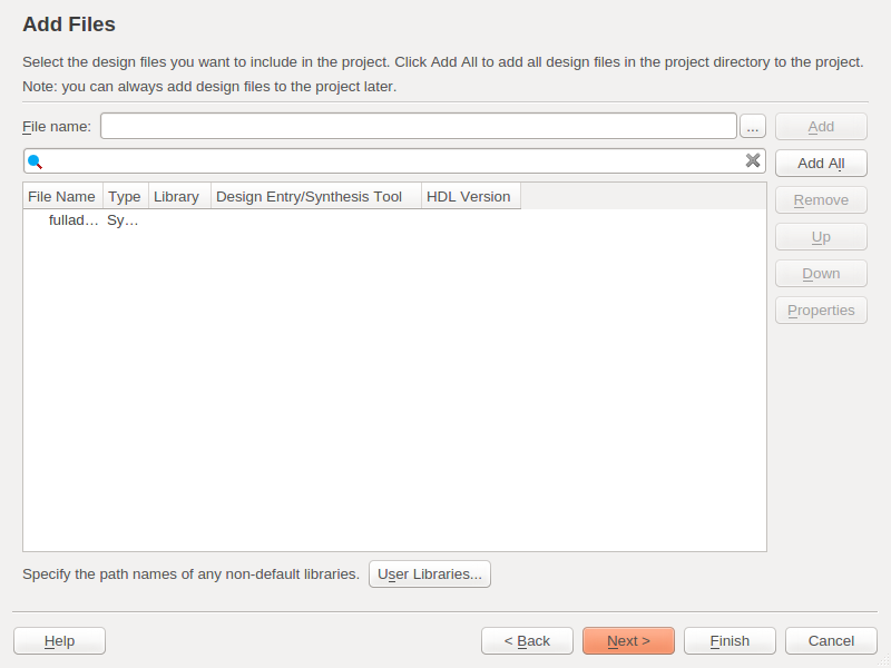
When you get to the screen to add files,
Click on the three dots just to the left of the
Add button, and
use the browser to select your
fulladder.v file.
Do not use the testbench program.
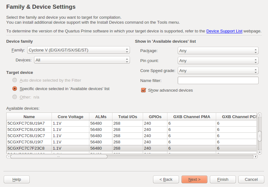
Just choose the first device you see. It will be something like
an 5CGXFCSCI320.
In the tool settings, change VHDL to SystemVerilog. (I doubt
this is really necessary.)
Use the defaults in the remaining screens.
With Processing ⇒ Start Compilation, you should now be able to compile and synthesize. Expect a long wait and lots of warnings.
Examining the results
Now just poke around a little.
Under Assignments, look at Pin Planner. There you will see how your five pins are mapped to the pins of the FPGA.
Close the Pin Planner window and return to the main Quartus window. Use Tools ⇒ Netlist Viewers ⇒ RTL Viewer to view the compilation of your SystemVerilog program to gates. Without closing the RTL Viewer window, use Tools ⇒ Netlist Viewers ⇒ Technology Map Viewer (Post Mapping) to view the compilation into the combinational logic cells of the FPGA.
The combinational logic cells are implemented by the LUT, or look-up table. The LUT is a multiplexer connected to SRAM, memory that is loaded when the FPGA is turned on. Take a look at Figure 3 on page 2 of Altera’s white paper on FPGA architecture to see how a LUT is implemented in silicon.