Solution CSCI 311 / ENGR 212 / ECE 212 Homework Assignment 8
Problem 1
Problem 1(a)
Draw the transistor-level structure for a single SRAM cell; do not show
the transistors inside the inverters (instead, use the inverter symbol);
be sure to label wordline and bitlines.
Explain how the cell is read and written.
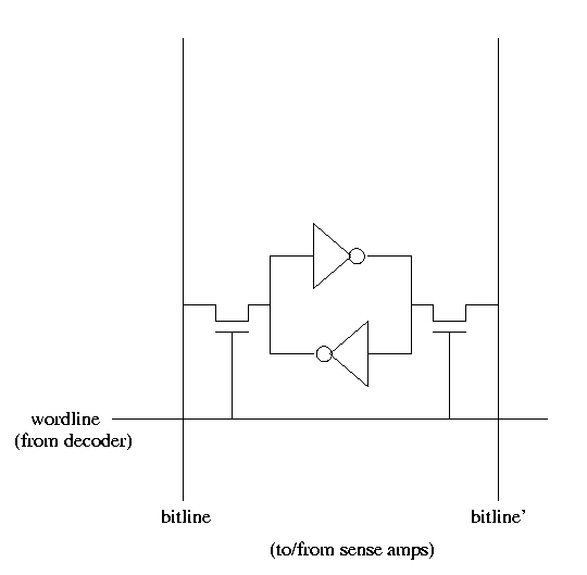
- READ and WRITE
-
Address is decoded by address decoder, causing a specific wordline
to be asserted. When the wordline of this cell is asserted, the two
pass-transistors switch on, connecting the cell to both bitline and bitline'.
What happens next depends on read or write, described below...
- READ
-
A differential sense amplifier connected to the ends of the bitlines
(not shown) reads the cell's value on the bitlines.
- WRITE
-
Write circuitry connected to the ends of the bitlines (not shown) forces a
value (0 or 1) on bitline and the complementary value (1 or 0) on bitline',
forcing the cell contents to a new state (or the same state, depending on what
is already stored in the cell). Note that during the process, the inverters
and the write circuitry are both driving the same node; the write circuitry
is designed to overpower the inverters to win the competition.
Problem 1(b)
Draw the transistor-level structure for a single DRAM cell and explain how
it is read and written. Make sure to label wordline and bitline.
When and why does a DRAM cell have to be refreshed?
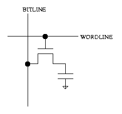
- READ and WRITE
-
Address is decoded by address decoder, causing a specific wordline
to be asserted. When the wordline of this cell is asserted, the single
pass-transistor switches on, connecting the cell to the bitline.
What happens next depends on read or write, described below...
- READ
-
If the cell contains a "1", that means the capacitor is charged and at a higher
voltage level than the bitline. If the cell contains a "0", that means the
capacitor is discharged and at a lower voltage level than the bitline.
So, depending on the value of the capacitor initially, when the cell is read,
charge either flows from the capacitor to the bitline (if it is 1) or from the
bitline to the capacitor (if it is 0). A sense amplifier connected to the
end of the bitline (not shown) senses a small change in charge on the bitline,
and also the direction of the change, indicating either a 0 or 1.
The problem with this approach is that the value stored in the capacitor
changes after reading, since reading involves a movement of charge to/from
the capacitor. So, reads are "destructive". As a result, just after reading
a cell, the value read out must immediately be written back to the cell.
I.e., a single read cycle is actually a read+write cycle. That is why,
in DRAM, reads take longer than writes. Writing is described below.
- WRITE
-
Write circuitry connected to the end of the bitline (not shown) pulls the
bitline up to a "1" voltage level or down to a "0" voltage level, depending
on the value being written. This either charges or discharges the cell's
capacitor, storing either a 1 (charged) or a 0 (discharged), respectively.
(Unlike the active inverter devices in the SRAM cell, the DRAM's capacitor
does not "fight" the write circuitry since it is a passive device.)
- REFRESH
-
Cells have to be refreshed (1) immediately after being read and
(2) periodically (e.g., every 64 ms) due to unavoidable leakage current
from the capacitor. The capacitors lose their charge over time, through the
leaky pass-transistor. Fortunately, 64 ms (64 milliseconds) is a very long
time from the perspective of a computer, which today operates at a frequency
of 1-3 GHz (<1 nanosecond period -- 1 million times faster than refresh rate).
Also, processors access main memory much less frequently than its on-chip
caches, so the DRAM bandwidth stolen from the processor in order to do refresh
operations does not degrade performance all that much.
Problem 1(c)
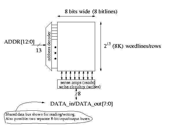
Draw a high-level block diagram of the internal organization
of an 8K x 8 SRAM. Do not be concerned with details -- the idea is
to show the dimensions of the SRAM and the widths of "buses".
- Show the memory storage array as a single box with width/height
dimensions labeled.
- Show the address decoder block, with the address bus coming in (label
with the width of the bus) and wordlines coming out (no, don't draw
all wordlines, just give the general idea).
- Show the data bus (label with the width of the bus), i.e., bitlines,
coming out of the memory structure.
Problem 1(d)
Fill in the following table with "yes" or "no" in each box.
| | Flash and EEPROM | SRAM | DRAM |
|---|
| non-volatile | YES | NO | NO |
| periodic refresh required | NO | NO | YES |
| destructive reads | NO | NO | YES |
| relatively slow but very dense | leave blank | NO | YES |
| relatively fast but not very dense | leave blank | YES | NO |
| typically used for main memory | NO | NO | YES |
| typically used for processor caches and register files | NO | YES | NO |
| typically used to assist booting or to store configuration information | YES | NO | NO |
Problem 2
Show how to build a 512x8 ROM out of 64x16 ROM chips and
appropriately sized decoders.
Assume that the ROM chips you use in this problem have
OE (output enable)
and CS (chip select) inputs.
Be sure to clearly label the address and data output
connections of your solution.
Because (512x8)/(64x16) is 4, you'll need four 64x16 ROM chips
to implment the 512x8 ROM. Since
word size than the 64x16 ROM, you'll need a 8-bit wide 2-to-1 MUX
to select 8 bits from the 16 produced by the 64x16 ROM.
The 64x16 ROM's are placed in "rows" containing one 64x16 ROM.
You'll need a 2-to-4 decoder do enable the correct row.
Since log2 512 is 9, the 512x8 ROM requires
nine address bits. The two most significant address bits are connected
to the 2-to-4 decoder. The least signifcant address bits is connected
to the single selector input of the 2-to-1 MUX.
This leaves six address bits to connect to the address lines of
the 64x16 ROM's. Since log2 64 is 6, all is well.

Problem 3
Implement the following functions using 16x1 ROMs:
-
f1 = Σ(0,1,2,6,7,9,11) and
f2 = Σ(0,1,3,4,11,12,15):
Show the labels for the inputs and outputs, and the content of ROM.
Just fill up two ROM according to the truth table.
-
A Mealy machine sequence detector that detects overlapping sequence
'010':
Show the state transition diagram, state assignment, state table,
and the circuit that consists of D flip-flops and the memory
(with its content).
There are many possible answers depending on your
state assignment.
| state | input |
|---|
| 0 | 0 |
| S |
S0/0 |
S/0 |
| S0 |
S0/0 |
S01/0 |
| S01 |
S0/1 |
S/0 |
| state |
|---|
| logical | binary |
|---|
| S | 00 |
| S0 | 1- |
| S01 | 01 |
| state |
I |
state |
O |
| Q1 |
Q0 |
Q1* |
Q0* |
| 0 |
0 |
0 |
1 |
- |
0 |
| 0 |
0 |
1 |
0 |
0 |
0 |
| 0 |
1 |
0 |
1 |
- |
1 |
| 0 |
1 |
1 |
0 |
0 |
0 |
| 1 |
0 |
0 |
1 |
- |
0 |
| 1 |
0 |
1 |
0 |
1 |
0 |
| 1 |
1 |
0 |
1 |
- |
0 |
| 1 |
1 |
1 |
0 |
1 |
0 |
This time you'll need three ROMs, two for the flip-flop inputs and one for
the state machine output. Only eight rows of the ROM need to be filled.
Problem 4
For the following caches, determine the number of cache blocks.
Also, partition and label a 32-bit address into the block offset field,
index field, and tag field for the caches.
-
8KB direct mapped cache, with a block size of 64 bytes.
The number of block offset bits is log2 64 or 6.
The number of cache blocks is 8k/64 or 128. Consequently, the number
is of index bits is log2 128 or 7. The number of
tag bits is 32-7-6 or 19.
16KB direct mapped cache, with a block size of 32 bytes.
The number of block offset bits is log2 32 or 5.
The number of cache blocks is 16k/32 or 512. Consequently, the number
is of index bits is log2 512 or 9. The number of
tag bits is 32-9-5 or 18.
Problem 5
Apply the following address stream to a 256 byte direct mapped cache,
with block size of 16 bytes.
The number of block offset bits is log2 16 or 4.
The number of cache blocks is 256/16 or 16. Consequently, the number
is of index bits is log2 16 or 4. The number of
tag bits is 32-4-4 or 24.
- 0xfffec441
- 0x07395a20
- 0x00ee0224
- 0xbadbee44
- 0x000099c0
- 0x000099c8
- 0xffffffc4
- 0xbadbee4c
The following table shows what happens when the addresses are applied in
sequence:
| address | tag | index | comments |
|---|
| 0xfffec441 | 0xfffec4 | 0x4 | Miss |
| 0x07395a20 | 0x07395a | 0x2 | Miss |
| 0x00ee0224 | 0x00ee02 | 0x2 | Miss, replace 0x07395a |
| 0xbadbee44 | 0xbadbee | 0x4 | Miss, replace 0xfffec4 |
| 0x000099c0 | 0x000099 | 0xc | Miss |
| 0x000099c8 | 0x000099 | 0xc | Hit |
| 0xffffffc4 | 0xffffff | 0xc | Miss, replace 0x000099 |
| 0xbadbee4c | 0xbadbee | 0x4 | Hit |
-
Show the final contents of the cache. Only show the tags.
Leave cache blocks that were not touched by the address stream blank.
| block | tag |
|---|
| 0 | |
| 1 | |
| 2 | 0x00ee02 |
| 3 | |
| 4 | 0xbadbee |
| 5 | |
| 6 | |
| 7 | |
| 8 | |
| 9 | |
| 10 | |
| 11 | |
| 12 | 0xffffff |
| 13 | |
| 14 | |
| 15 | |
-
How many cache hits were there? (Assume the cache is initially empty.)
2
-
How many replacements were there? (Assume the cache is initially empty.)
3