


Write a VHDL behavioural specification for the majority function. Assume the input variables are X, Y, and Z and the output variable is M.
The answer should be a single line similar to:
A <= (X and Y) or (not X and not Y) ;M <= (X and Y) or (X and Z) or (Y and Z) ;Design a 4-bit binary counter that counts modulo-9 with the counting sequence:
Design this as a custom circuit using gates and flip-flops. That is, begin with a state table and synthesize the circuit from the state table. Exploit don't-care states if applicable. Use an external asynchronous RESET input to initialize the flip-flops to the initial state.
Repeat subproblem 2(a), but use a 74x163 as the basic building block, and add external logic to drive the counting sequence. Use an external synchronous input called init for initializing the counting sequence.

Which approach was easier? Which approach was less expensive? Explain your answer.
Approach (b) was certainly easier. It is also less expensive if the number of discrete chips and external wires determines the cost/size of the system. Part (a) requires two 7474 D flip-flop chips (four D flip-flops), and at least several 2-input/3-input NAND chips (convert AND-OR logic to NAND-NAND logic). Part (b) requires one 74x163 chip and one or two other chips (depending on exact implementation of the external logic… can map the logic onto a NAND chip). Another cost factor is the time needed to design a circuit: engineering effort. Approach (b) is certainly less costly in terms of engineer-hours.
Design a Mealy state machine to detect the sequence 10010. There is a single input x and a single output z. The output is set to 1 when the sequence is detected
Design the state machine using gates and flip-flops in the standard way, i.e., begin with a state diagram and state table, do plain state assignment (e.g., for three state variables, first state is 000, next is 001, and so on), use K-maps to derive minimized next-state and output equations (exploit don't-care states if applicable), and synthesize the circuit diagram from the equations.

Repeat problem 3(a), but this time use a shift register to design your circuit.
Which approach was easier? Which approach was less expensive? Explain your answer.
Approach (b) was certainly easier. It is also less costly and takes less space, in terms of discrete chips and external wires. The shift register design probably requires 3 chips: 2 7474 D flip-flop chips (four D flip-flops) and 1 3-input AND chip (two AND gates can form the 5-input AND logic), assuming complemented outputs of flip-flops are used instead of inverters at inputs of AND logic. The non-shift-register design would also use 2 7474 D flip-flop chips (5 states encoded with 3 flip-flops), plus several chips for next-state and output logic. Another cost factor is the time needed to design a circuit, the engineering effort. Approach (b) is certainly less costly in terms of engineer-hours.
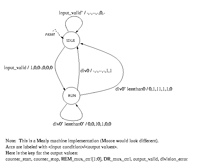
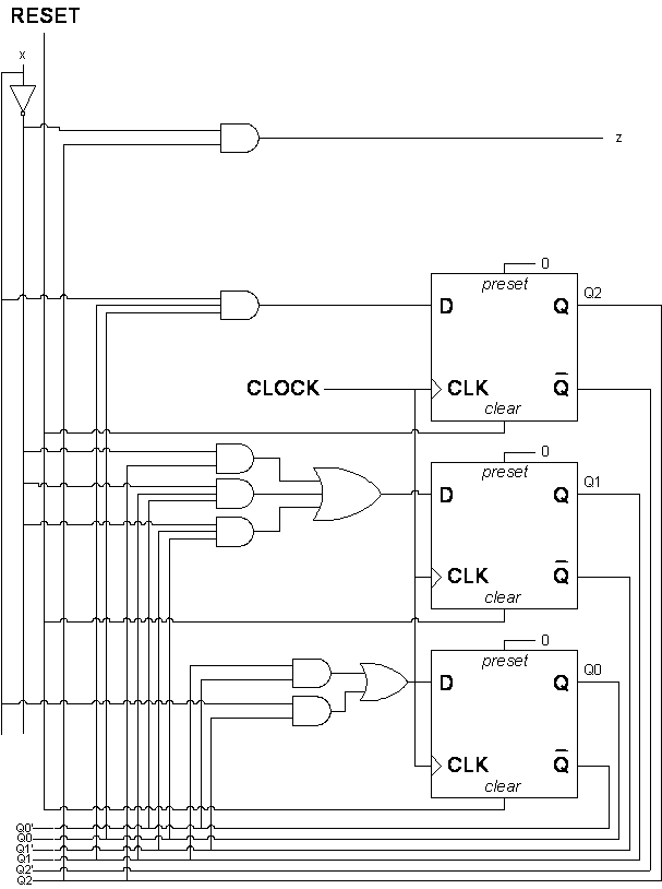
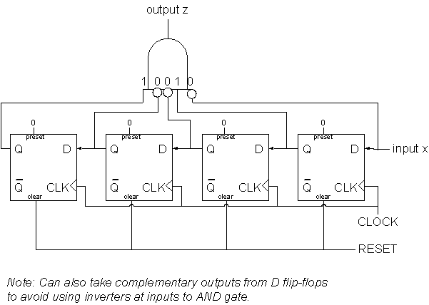
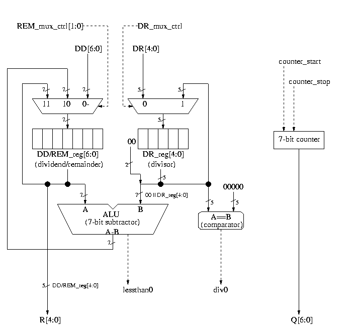
Design a division circuit that will divide a 7-bit number by a 5-bit number. You'll do the division by successive subtraction, continually subtracting the 5-bit number from the 7-bit number until no further subtractions are possible. You'll then report the quotient and remainder of the operation.
Your design should include the datapath unit and the control unit of the system and the signals that interact between them. Your final design should show:
Different solutions are possible, because of slightly different datapaths, timing assumptions, Mealy vs. Moore implementation, and design style. But the fundamental aspects of the datapath should be the same. Here is one possible solution...
Top-level diagram of the overall system
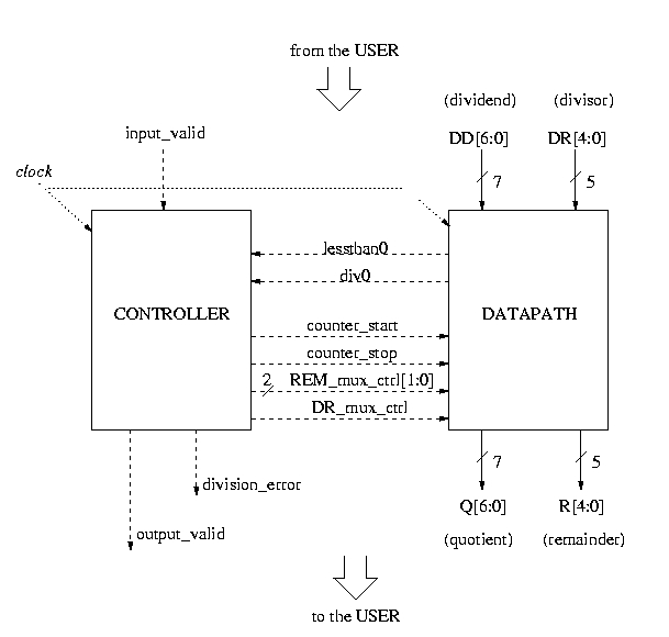
Block diagram of the datapath
State diagram for the control unit