This lab is scheduled for 20 & 21 March
First of all, thanks to Sally Medling of NCSU for generating the document from which part of this lab was constructed.
The purpose of this lab is to introduce you to breadboards, LED's, switches, and a few analog components used in digital design.
This is a very hands-on lab. It's not rocket science, but there are a lot of detailed work that must be done carefully. Take it easy and go slow.
You are going to build your circuit on a breadboard. The circuit will have four distinct sections.
The breadboard, or socket board, is an easy-to-use wiring chasis that contain lots of holes, or sockets, in which wires and components are inserted. The power and beauty of the breadboard derives from the fact that the sockets are connected by strips of metal running underneath the board. This allows you to connect components without burning your fingers with a soldering gun.
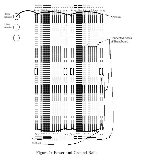
In the middle of the breadboard, you'll see a large number of small rows of five sockets. All five sockets in each row are connected to each other but not to the sockets of any other row. Along the outside of the breadboard, you'll see longer rows, or rails. All the sockets of each rail are connected. Use these rails to distribute power and ground to your circuit.
In the figure below (provided by the folks at NC State), the
connected rails and rows of a breadboard are shown. Note
that several wires have been added to circuit to make
rows W and Z into power rails and rows X and Y into ground
rails.
You will only need use the left side of the breadboard in this lab. Go ahead and wire the rails. I suggest you use red wire to connect the power rails and black wire to connect the ground rails. The rails along the long edge of the breadboard are actually disconnected in the middle. One very common mistake is neglecting to add a connection between these two "half" rails.
Below is a picture of how your breakboard should look once
you have added the power distribution wires.
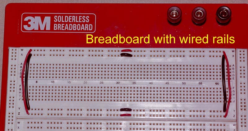
By the way, Iguana Labs has a Using the bread board (socket board) tutorial with some nice pictures and useful information. If you want your own breadboard, you can get one for about $10 at Radio Shack. Batteries are not included.
We'll be using TTL (transistor-transistor logic) chips in our lab. These chips want a nice regulated five volts. We'll use a 7805 voltage regulator which receives an unregulated six (or more) volts and produces a regulated five volts. Because we're careful, we'll also use a 10µF electrolytic capacitor to protect against voltage spikes on the five volt side of the circuit.
A schematic view of the voltage regulator "circuit" is shown
below:
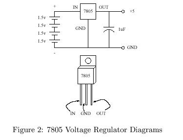
The electrolytic capacitor has polarity.
This means that you must connect the lead labeled with
minus sign to the lower voltage or, in this case, ground.
Front and back views of a correctly placed voltage regulator
and capacitor are shown below.
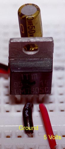
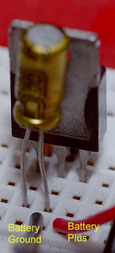
Place the 7805 and capacitor on the breadboard and have your lab instructor verify your work. Be sure that your capacitor is inserted correctly.
This circuit will only need two inputs. Each
implemented as follows:
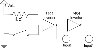
Your circuit needs switches for "entering" input. In a real circuit you'd use pushbuttons, but we're going to have you input bits by physically moving wires. If the wire is connected to ground, the input to the first inverter will be zero volts. Consequently, the output of the first inverter will be a logical 1 and the output of the second inverter will be a logical 0. If the wire is unconnected, the input to the first inverter will be five volts, provided through a 1kΩ resistor. In this case, the output of the first inverter will be a logical 0 and the output of the second a logical 1. The 1kΩ resistor has bands of brown, black, and red. If you don't know the resistor code, try out Danny Goodman's JavaScript resistor calculator.
Note that our two switches actually produce four logical values in two complemented pairs. We'll call these values X, X', Y, and Y'.
We'll use a single 7404
hex invertor to implement all
four invertors needed by this part of the circuit.
The 7404 has fourteen pins that are numbered
counter-clockwise starting with the notch.
The pin to the left of the notch is number 1.
The chip's ground connection will always be in the lower-left
corner, and its power connection will
in the upper right corner, just to the right of the notch.
For the 7404, pin 7 is ground
and pin 14 is power.
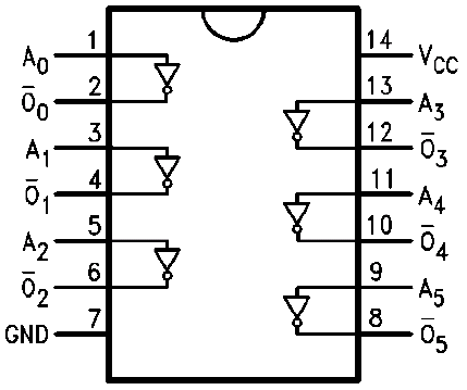
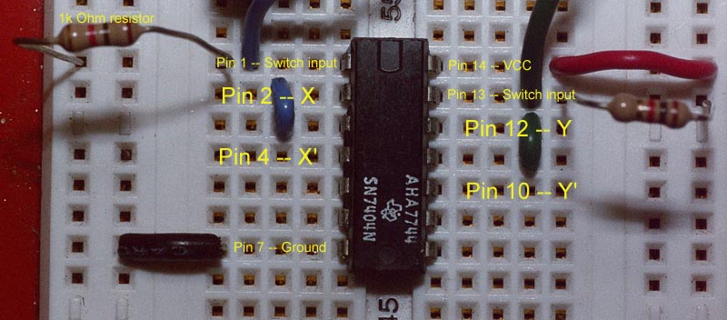
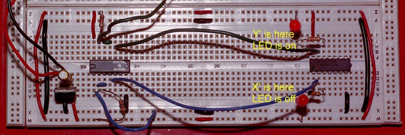
If you wire your circuit as shown in the following picture,
logical variable X is produced on pin 2 while
its complement X' is produced on pin 4.
Similarly, logical variable Y is produced on pin 12 while
its complement Y' is produced on pin 10.
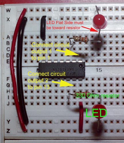
You will view the logical outputs of your circuit on LED's. We wish for the LED to be lit when the output is 1 and to be off when the output is 0. We will use a 7405, or hex inverter with open-collector outputs, for this task. The pin connections of the 7405 are identical to those of the 7404.
A schematic for each LED output circuit is shown below:
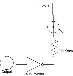
When the input to the circuit is 1, the output of the invertor
will be 0. This will sink current through the
LED and turn it on. A 330Ω current limiting resistor
is used to restrict the current
flow through the LED to about 10 mA.
The 330Ω resistor has bands of
orange, orange, and brown.
You can still review
Danny Goodman's JavaScript resistor calculator.
Because LED's are diodes, they have an anode and cathode. The LED will conduct only when the anode is connected to a higher voltage than the cathode. If you look at an LED from above, you'll see a circle with a flat spot. The flat spot marks the cathode. The cathode wire should also be a bit shorter than the anode wire. The LED's must be inserted into the breadboard with the anode connected to VCC.
Now wire up your 7405 for two outputs
as shown in the following picture.
Use long pieces of wire to connect each of the outputs of
your switch circuit to the inputs of your LED circuit.
Use your switch wires to make sure that your LED and switch
circuits are working properly.
Finally, it's time for some thinking. Way back in Lab 2 you implemented, in the Multmedia Logic Simulator, the two functions are given in the following table:
| X | Y | F | G |
|---|---|---|---|
| 0 | 0 | 0 | 1 |
| 0 | 1 | 1 | 1 |
| 1 | 0 | 0 | 0 |
| 1 | 1 | 0 | 1 |
Just in case you've forgotten, the functions were originally expressed as:
Then by application of de Morgan's law, they were implemented with NAND's and NOT's as:
Using the outputs of your switch circuit, you are to implement these two functions with a single 7400 chip, a collection of four 2-input NAND gates. Note that your task is to simultaneously implement both functions with one chip. Implementing one function and then the other is not good enough.
The 7400
is a quad 2-input NAND gate whose connection diagram
is shown below:
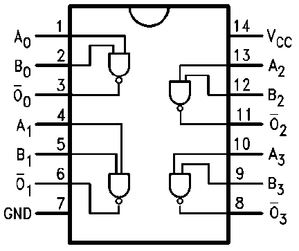
Your switch circuit will provide you with X, NOT(X), Y, and NOT(Y). Draw a diagram of show how to wire up the 7400 to implement F and G. By the way, it's not hard to implement a NOT by using a NAND.
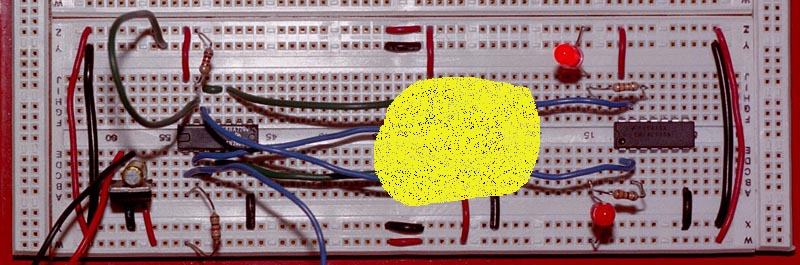
Have the lab instructor verify your wiring plan and then start wiring up the circuit. Finally, demonstrate that your circuit works for all four input combinations.
Here's a picture of a working circuit.
Unfortunately there's a yellow blob obscuring the 7400.
Tear down your circuit and give it to the lab instructor. Whew.