Again, you can do this lab in groups of two or three. We're interrupting our "Circuits in SSI" series to take a look at some of the modules described in chapters 5 and 7 of the textbook. This lab is a bit of an extension of Homework 1 and the beginning of Homework 2.
Download our ZIPed copy of diglog and a ZIPed copy of a diglog input file and install it into
In this lab we're going to begin to implement the Syracuse problem described in Homework 1 using 4-bit adder, 4-bit multiplexers, and 4-bit register. First, of all, remember the Syracuse function:
long nextnum(long x) {
  if (x % 2 == 1)
    x = 3*x + 1 ;
  else
    x = x/2 ;
  return(x) ;
}
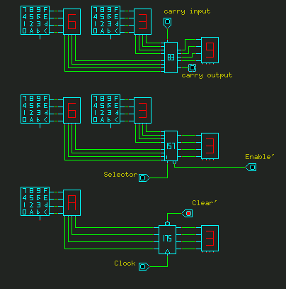
Start up diglog and load in the file lab7play.lgf. Note that this circuit uses the following three "Digital TTL gates".
Your first task is to "play" with these circuits and to demonstrate to the instructor that you understand how to control them. Before calling the lab instructor, you must:
Create a new circuit containing one register, one adder, and two seven segment displays. Next connect the outputs of the register and the adder to the two (different) seven segment displays.
Now it's time for the tricky part. Connect the output of the register to the inputs of the adder, so that if the register contains the value x, the output value of the adder will be (3*x + 1) mod 16. Hint: 3*x is (x<<1) + x.
Show your completed circuit to the lab instructor.
Now let's put this circuit into a loop. Connect the outputs of the adder to the inputs of the register. Add a clock and a clear input to the register. Clock the circuit a few times. It should cycle through the hexadecimal numbers 0, 1, 4, d, 8, 9, C, 5, and back to 0. This is your first sequential circuit. Show it to the lab instructor.
Now let's allow the "user" of the circuit to "input" an arbitrary starting point for our calculation. Add a selector and a hexadecimal keyboard to your circuit. Connect the outputs of the selector to your register; connect the outputs of the adder to one input set of the selector; and connect the outputs of the keyboard to the other selector input set. Finally, add a control input to the selector so that the selector can be loaded from either the adder or the keyboard. Show the completed circuit to the instructor.
FTP a copy of your completed circuit to the file ~/csci/255/lab7.lgf on the CSCI workstations. You'll extend this circuit in Homework 2. Go ahead and work on Homework 2 if you wish.
Return to CSCI 255 home page.