This lab was designed by Wayne Lang.
Being magic with the spell
Make a rectangle on the screen by pressing first with the left button (lower left corner) and then moving the cursor to upper right and press with the right button.
Make the text window small and at bottom of screen. Make the graph window large but do not cover text window.
Make a rectangle of red by typing
in the text window
Now make a rectangle of blue. Press the left button at another point on screen and then type
in text window
Make another rectangle of red by moving rectangle to new place, placing the cursor over the red area, and pressing the center button.
Delete a red rectangle by surrounding the rectable with a white box. Type
and it will be gone
Load a new file by typing in the text window
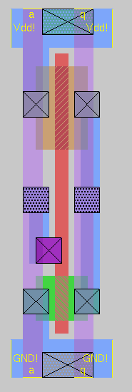
The file i1s.mag is a
specification of the following CMOS inverter:
Surround the inverter circuit with white box. Press z to zoom the circuit up to the full size of your picture screen. Press Z to zoom down in size.
Now let us "reverse engineer" this thing. That is, we will take off one layer after another starting from the top. As you remove each layer be careful to note where that layer is selected. Label this item on your handout pictures. Magic looks straight down at the top of the chip.
Surround the circuit with the white box and type
you will see the purple stuff selected. Now we delete the metal2 layer
Select and delete the blue metal1 are by typing
The via is a connection between the upper metal2 layer and the metal1 layer that is directly below it. Remove the via with
to remove the via boxes.
Now take away the poly layer.
The connector block joins poly and metal1. The layer is called "pc". Remove it.
Now we're going to work on the N-channel transisitor. First remove the n-diffusion (or "ndiff") area. Note that this does not remove the n-channel that is under where the poly crossed the n-diffusion area.
Remove the n-channel, called "nfet".
Dispose of the P-channel transistor by removing the P-diffusion (pdiff) layer thand then the active transistor (pfet).
Remove "ndc", the connection between the metal1 and the P-diffusion layer and "ppc", the P-layer substrate connection, and "nnc", the N-layer substrate connection.
Finally, type
for a more complete description of the layers.
Return to CSCI 274 labs
Return to CSCI 274 home page
Return to Dean Brock's
home page
 Return to the UNCA Computer Science home
page
Return to the UNCA Computer Science home
page