Getting ready
You’ll need the follow hardware for this lab.
- Breadboard — large or medium
- Three resistors — 1k Ω
- Three LED’s: green, yellow and red
- Two push-down switches
- A small amount of wire
- Microstick II
Microchip references
- PIC32 Family Reference Manual (Documentation → Reference Manual)
- PIC32 Family Reference Manual, Sect. 12 I/O Ports
- PIC32MX1XX/2XX 28/36/44-PIN datasheet
- Microstick II
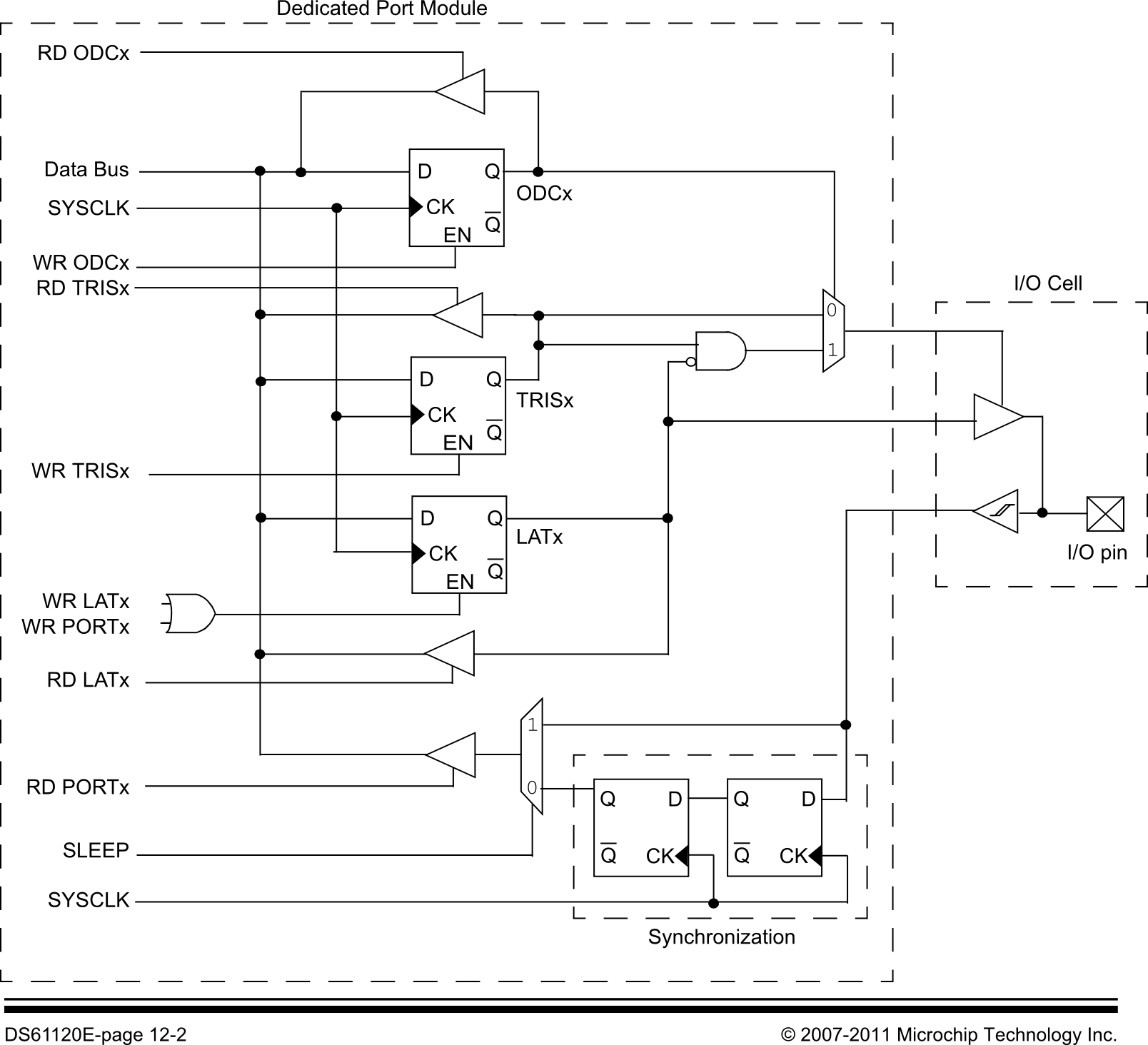
Pin I/O and the special function registers
On the PIC32 microcontroller there are a few special function registers (SFR’s) that are used for pin I/O. Some of these registers change the pins. Others configure the pins. The SFR’s are used just like memory locations: except that reading from and writing to them performs magic operations on the pins.
Most pins of the chip can be configured for several different modes of operation. Configuration is done by setting bits within special file registers dedicated to pin I/O configuration.
The GPIO pins are divided into sets called ports, each
having its own set of SFR’s.
This division will seem very arbitrary.
On the PIC32 microcontrollers
you will be using,
Port A has five ports,
RA0 to RA4, while Port B has fourteen ports,
RB0 to RB5,
RB7 to RB11, and
RB12 to RB15.
To keep things simpler we will only use the Port B pins.
Still you will need a diagram to figure out
where the specific pins are located.
A diagram for the chips we’ll be using is found on
page 5 of the
PIC32MX1XX/2XX 28/36/44-PIN datasheet.
The SFR’s used to control the pins are known by special names,
such as TRISA and TRISB. Note the
are different names for the two ports.
In PIC32 documentation, the name TRISx
will be used to refer to either the
TRISA and TRISB SFR.
Each SFR has a unique address.
The C prototype for TRISA is found in the
compiler include directory, in our case
/opt/microchip/xc32/v1.40/pic32mx/include/proc,
in files, such as p32mx250f128b.h.
There you will find unusual declarations such as:
extern volatile unsigned int TRISA __attribute__((section("sfrs")));
for the SFR’s. (By the way, Java also uses the modifier
volatile for a similar purpose.)
The TRISA SFR has the virtual
address 0xBF886010. That information is found in
one of the many processor.o files distributed
with the compiler.
If you really want to find the compiler definitions for all the
SFR’s, you can try out something like the following command:
/opt/microchip/xc32/v1.40/bin/xc32-objdump -t \
 /opt/microchip/xc32/v1.40/pic32mx/lib/proc/32MX250F128B/processor.o
Whew.
Characteristics of Pin I/O
For now we are going to look at a small subset of the many functions that can be performed using the pins of the PIC32 microcontroller. Because this subset is adequate to get us through the first few labs, we’re going to pretend that the pins are limited to the following characteristics during this lab.
Digital or Analog
Most, but not all, pins can be used as either digital or analog interfaces. When used for digital I/O, they interpret 0 v as 0 and 3.3 v as 1. When used for analog input, a 16-bit value giving the input voltage level at a pin is provided by the chip. Analog output is a much more complex and depends on PWM (Pulse Width Modulation), a concept that will be introduced in this lab and discussed more fully in a future lab.
The ANSELx registers are used
to configure each pin as digital or analog.
By default, pins are analog. That is a bit unexpected.
Writing 0 sets the pin to digital.
In this lab description, we’ll follow the Microchip practice of
referring to the related pair of special function registers as
ANSELx.
Input or Output
A digital pin can be used for either input or output.
By default, digital
pins are set for output when the pin is configured for
digital I/O using ANSELx.
The input or output setting is
controlled using the TRISx registers.
“TRIS” is an abbreviation for
TRI-STATE®, a registered trademark of National Semiconductor.
Writing 0 (looks like ‘O’ for output) sets the pin to digital.
Writing 1 (looks like ‘I’ for input) sets the pin to digital.
Microchip recommends that unused pins be set to digital output with low written to the pin. This is something we will do in our labs.
Change notification
Pins can be set to interrupt the processor when an input to the chip is changed by an external circuit. This allows the chip to “sleep” and plays a significant role in reducing battery life in consumer devices.
Change notification is enabled
using the CNENx registers.
Weak pull-ups and pull-downs
“Weak” pull-ups and pull-downs can be enabled on pins. When a pull-up is enabled, an input pin reads as 1 when no external voltage source is “driving” the line connected to the pin. To avoid the cost of an external resistor, weak pull-ups are often used when pins are connected to push-button switches.
When a pull-down is enabled, an input pin reads as 0 when no external voltage source is connected to the pin.
The pull-ups and pull-downs are enabled
using the CNPUx
and CNPDx registers.
The PIC32 documentation states that weak pull-ups
and pull-downs should be disabled
when a pin is used for digital output.
This could be your only UNC Asheville class where pull-ups are discussed.
Open-drain
Some digital output pins can be set to “drain” their lines. An open-drain pin can “sink” current on a output line until 0 v is reached or it can allow the output to “float” to an externally set value, which might even be higher than 3.3 v.
Open drain is enabled using the ODCx
registers; however, the
drain is switched on and off using the TRISx registers.
Writing to a digital pin
Digital output pins are written using the
LATx latch registers.
The LATx registers store the output values
that are being written to the external world.
It is similar to a D-latch.
If a pin is configured for input, the
LATx and PORTx
registers can differ. Also, it can take
a few microseconds for values written to the LATx
register to be reflected in the PORTx registers.
Reading a digital pin
The values of the digital input pins are read using the
PORTx registers.
Do not write to these registers!
How it all looks
Writing to GPIO registers
Here’s some C code that will initialize all the GPIO pins to be digital output pins.
    ANSELA = 0 ;           // Set all pins for digital
    ANSELB = 0 ;
    CNENA = 0 ;            // Disable change notification
    CNENB = 0 ;
    CNPUA = 0 ;            // Disable weak pull-up
    CNPUB = 0 ;
    CNPDA = 0 ;            // Disable weak pull-down
    CNPDB = 0 ;
    ODCA = 0 ;             // Disable open drain
    ODCB = 0 ;
    TRISA = 0 ;            // Set all pins for output
    TRISB = 0 ;
    LATA = 0 ;             // Write 0 to output
    LATB = 0 ;
Each of these registers has a bit devoted to a specific pin. In particular, the i’th bit of the register controls the i’th pin of the port.
If you want to write a 1 to port RB11 and not modify
the other pins of Port B, you need the following line of code:
LATB = LATB | 0x00000800 ;
0x00000800 is a literal with only its eleventh bit turned on.
Similarly to write a 0 to port RB11 without modifying other pins,
you need
LATB = LATB & 0xFFFFF7FF ;
which would be clearer if written as
LATB = LATB & ~(0x00000800) ;
However, the proffered style is the C idiom
LATB = LATB & ~(1<<8) ;
To make PIC32 code easier to write there are three additional SFR’s
for each of the SFR’s mentioned above. To write a 1 to only one
port use
LATBSET = 0x00000800 ;
To write a 0 to only one port use
LATBCLR = 0x00000800 ;
(Yes, you do write a one to store a zero.)
And finally, if you want to toggle an output bit
LATBINV = 0x00000800 ;
By the way, the computers chips used in both the Arduino and Raspberry Pi have similar sets of registers for manipulating GPIO pins.
The downside of multiple usage
Unfortunately, a single physical pin has several names,
each reflecting a potential function.
For example, physical pin 6 corresponds to analog pin 4
(AN4) and GPIO port B
pin 2 (RB2).
It also happens to be known as
C1INB, C2IND, RPB2, SDA2,
CTED13 and PMD2.
That’s eight possible uses for one pin.
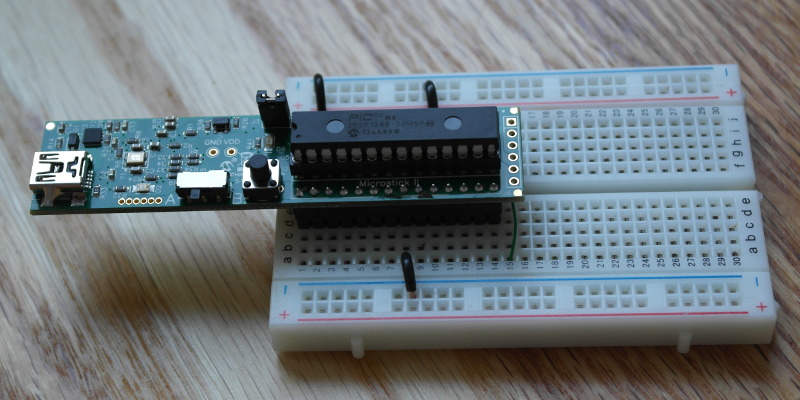
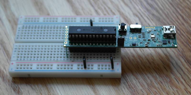
Back to the breadboard
We are are going to complete this lab using a Microstick II with an MX250F128B chip. The Microstick will be placed in a breadboard for wiring components. (If you want to try the lab with an MX220F032B chip on a breadboard with a Pickit 3, ask the instructor how this could be done.)
The Microstick allows access to almost all pins of the MX250F128B; however, the regulated 3.3 v power supply is not available for external use. This places some restrictions on what we can do today. When we need power, we will have to add a voltage regulator to the breadboard.
In this lab your chip will
use two push-down switches for input and three LED’s as output.
The LED’s will be arranged to look a little like a stoplight.
The switches will be connected to pins 16 (RB7)
and 17 (RB8) of the Microstick.
LED’s will be connected, through resistors, to pins 11
(RB4) and 14 (RB5).
Microstick meets breadboard
Go ahead and carefully place your Microstick on the breadboard. The gold-plated pins on the Microstick are very fragile, so do not insert the Microstick until you are certain it is properly aligned. Arrange it so that pin 1 of the Microstick is in row 1 of your breadboard. This means that your Microstick will be occupying rows 1 to 14 of your breadboard and the USB interface of the Microstick will be hanging off the board. (Many of the larger breadboards use different numbers on the two edges of the breadboard. Use the numbers on the right side.)
Take a look at page 2 of the Microstick Information Sheet. You need to wire the ground pins of the Microstick to the ground rails of the breadboard. This means running black wires from pins 8, 19, and 27 of your Microstick to the breadboard grounding rails.
The numbering of pins on the Microstick follows pin numbering standards
of dual
in-line package (DIP) circuits.
The “top” of the chip is the short end with the notch.
Pins are numbered counter-clockwise starting with the pin just to the
left of the notch.

Run the ground connections for your Microstick II on the
breadboard and carefully place the Microstick on the board.
It should like something like the following pictures.
Or maybe, when you are done, a bit like crudely drawn image.
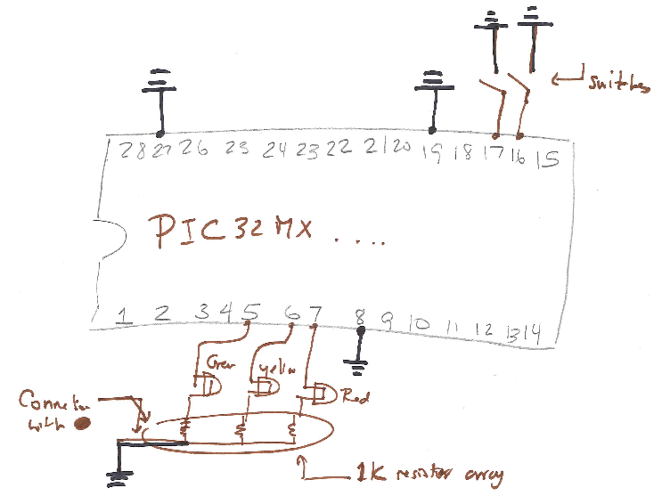
Adding lights and switches
Next you are going to connect three LED’s into your circuit. The LED’s should be run in series with a 1k Ω resistor between the Microstick and ground. If you don’t remember how to do this, you need to review the Adafruit lesson on digital inputs.
Wire the LED’s and resistors so that pin 7 connects to the green LED, pin 6 connects to the yellow LED, and pin 5 connects to the red LED.
Now it is time to connect the push-button switches. Again, if you don’t remember, review the Adafruit.
Connect your left switch to pin 17 and your right switch to pin 16.
Carefully make the connections, compare them with at least one other student, and let the instructor have a quick look at your work.
To review, your circuit should be wired up as specified in the table below.
| Circuit element | Microchip pin | Microchip port |
|---|---|---|
| Red LED | 5 | RB1 |
| Yellow LED | 6 | RB2 |
| Green LED | 7 | RB3 |
| Right switch | 16 | RB8 |
| Left switch | 17 | RB7 |
Programming the Microstick
In the world of embedded system development, programming refers to the process of downloading a program into the microcontroller.
Getting the hardware ready
Remove the Microstick from your breadboard, make sure your Microstick is not connected to the USB cable, and verify that your Microstick contains a PIC32MX250F128B microcontroller. If the Microstick does not contain a PIC32MX250F128B, replace the PIC microcontroller in the Microstick with a PIC32MX250F128B.
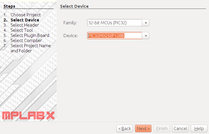
Starting the project
Start mplab_ide and create a project just like you have done in recent labs. When it comes time to choose the hardware device, select the PIC32MX250F128B that is on your Microstick.
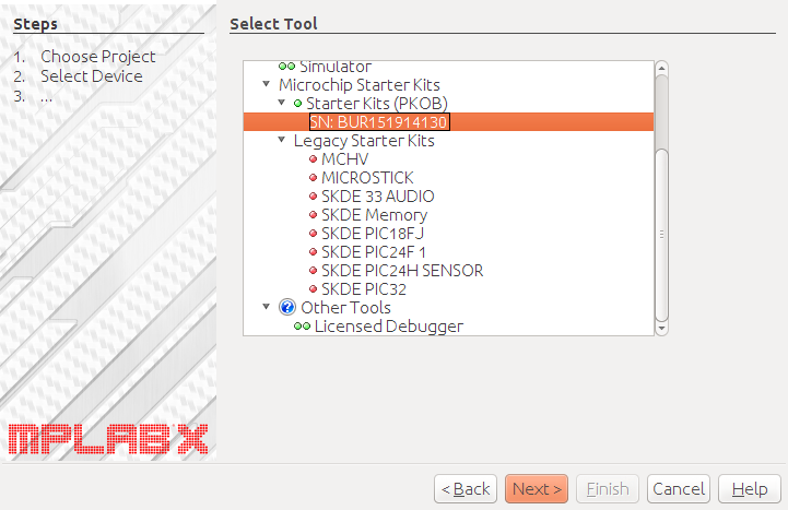
When it comes time to select your tool, choose the serial number
listed under Starter Kits.
You may want to verify that the serial number matches the one on your
Microstick.
Creating the program
Add a C main program to your project containing the following C code.
/*
 * File:   CSCI 255 Stoplight lab
 * Author: Your Name here
 */

#pragma JTAGEN=OFF
#pragma FWDTEN=OFF
#pragma FSOCEN=OFF

#include <xc.h>
#include <stdlib.h>

/*
 * Pins used in lab all on port B
 *   Pin  5 --  RB1  [PGEC1/AN3/C1INC/C2INA/RPB1/CTED12/PMD1/RB1]
 *   Pin  6 --  RB2  [AN4/C1INB/C2IND/RPB2/SDA2/CTED13/PMD2/RB2]
 *   Pin  7 --  RB3  [AN5/C1INA/C2INC/RTCC/RPB3/SCL2/PMWR/RB3]
 *   Pin 16 --  RB7  [TDI/RPB7/CTED3/PMD5/INT0/RB7]
 *   Pin 17 --  RB8  [TCK/RPB8/SCL1/CTED10/PMD4/RB8]
 */

/* All on port B */
#define GREENLED    3
#define YELLOWLED   2
#define REDLED      1

#define LEFTSWITCH  8
#define RIGHTSWITCH 7

void spin(int wastetime) {
    int i ;
    for (i=0; i<wastetime; ++i) ;
}

int main(void) {

    ANSELA = 0 ;           // Set all pins for digial
    ANSELB = 0 ;
    TRISA = 0 ;            // Set all pins for output except for SWITCHES
    TRISB = 0x0180 ;
    CNENA = 0 ;            // Disable change notification
    CNENB = 0 ;
    CNPUA = 0 ;            // Disable weak pull-up except for SWITCHES
    CNPUB = 0x0180 ;
    CNPDA = 0 ;            // Disable weak pull-down
    CNPDB = 0 ;
    ODCA = 0 ;             // Disable open drain
    ODCB = 0 ;
    LATA = 0 ;             // Write 0 to output
    LATB = 0 ;

    while(1) {
        spin(100000) ;
        LATBINV = 0x000E ;
    }
    return (EXIT_SUCCESS);
}
Build the program to make sure there are no compiler errors.
Programming the chip
Use the
Make and Program Device
icon
![]() to program your PIC32 processor.
You should get the message Programming completed
if this works.
However, if the firmware on the Microstick II hasn’t been
used in a while, it will be upgraded.
This can take quite a while.
Many lines will be output by the programmer
during this process.
to program your PIC32 processor.
You should get the message Programming completed
if this works.
However, if the firmware on the Microstick II hasn’t been
used in a while, it will be upgraded.
This can take quite a while.
Many lines will be output by the programmer
during this process.
Now slowly and carefully place your PIC32 into the breadboard. Remember that the pins on the Microstick are fragile, so be careful. This program just flashes the flights off and on.
Demonstrate that your program is flashing all three signals.
Programming with a bit more style
This program has awful style. Let’s try to fix it up a bit.
Eliminating magic constants
Start by getting rid of the magic constants
0x0180 and 0x000E.
Do this by defining masks for the bits.
Here an example of an appropriate mask.
#define GREENLEDMASK (1 << GREENLED)
It defines a bit mask that has a 1 in just the right place.
Add appropriate #DEFINE statements for all three LED’s
and both switches.
Use these defined constants to eliminate the magic constants.
You will probably need to use the logical or, |,
in your program.
Why not use const, rather than #DEFINE?
Well, because this is C. If this was C++, it might have
been better to use something like
static const int GREENLEDMASK = (1 << GREENLED) ;
which is also legal in C.
But in C this just isn’t the usual practice.
(Though, you are welcome to use it in this case.)
By the way, in C and C++ static has a very different meaning
than it does in Java.
Using standard library routines
With the Arduino, we were able to use calls like
pinMode
to set a pin to input and output or
digitalWrite to set the output value of a pin.
The Atmega chips used in the Arduino do have ports that contain several pins, just like the PIC; but the designers of Arduino chose the hide ports from most programmers. (See the picture of Arduino pin mappings to see how this is done.)
There is a
PIC32 peripheral library which contains several useful routines
for manipulating ports; however, it is a little hard to see much advantage
in using
PORTToggleBits(IOPORT_B, BIT_3|BIT_2|BIT_1) ;
rather than a simple write to LATBINV.
We could use the PIC32 peripheral library, just like we did last year, but Microchip is in the process of replacing the peripheral library with a new development system called Harmony which we will use in CSCI 320.
Doing a better job of keeping time
Take out a watch and count the number of times your light changes
in 100 seconds. (That will be two counts per flash.)
Use that count to adjust your argument to spin so that
the light changes about once a second.
Compare your count with your neighbors. The numbers should be close. If you are way off, try again.
Also add a #define”ed constant called
SPINSPERSECOND with the number you just discovered.
Use it in your program to make the lights change every second.
Finally a stop light
Modify your program that is acts a bit like a traffic signal; however, don’t make the lights stay on as long as a real traffic signal. That would be very boring.
Remember, the traffic signal goes green-yellow-red and the yellow is shorter than the green and yellow phases.
Another encounter with PWM
Try speeding up the traffic signal by modifying the argument passed to
spin. Make it 16 times faster, then 256 times faster, then
4096 times faster. Use one of the ugliest operators in
C (and Java)
the right shift assignment operator, >>=,
to avoid division.
A some point the LED’s will blink so quickly that your eyes cannot tell that the LED is flashing on and off. It should be the case that the yellow LED will be dimmer than the red and green. (Your mileage may vary. Some LED’s are just brighter than others.) This is an example of pulse width modulation (PWM), turning a digital output off and on so quickly that it looks like an analog signal. PWM is used to control motors and speakers, which are motors for moving air.
Right now, the yellow LED should be on about 10% of the time while the red LED should be on about 50% of the time. To make the difference a bit more noticeable, modify your code so that the red and green LED’s are on 90% of the time and the yellow LED in on 10% of the time, This will require some recoding inside your loop.
Show off your dimmed lights.
Because some LED’s are brighter than others and because our eyes perceive some colors easier than others, it may be necessary to use three cheap red LED’s in this experiment, rather than the more colorful LED’s. If you do this the LED in the middle should be dimmer than the others.
Finally the switches
Because we don’t have access to 3.3 V from the Microstick, we must use our switches in pull-up mode. This means the switches will be open when they are not pressed and will be close when they are pressed. Consequently, a switch will read as 0 when pressed and as 1 when not pressed.
Also, when reading the value of the switch, you should read the SFR
PORTB rather than LATB.
Before going any further, think about the tests you would use to
check if the switches are pressed.
Modify your code to accomplish the following: When the left button is pressed, the green and yellow LED’s are on. When the right button is pressed, the yellow and red LED’s are on. When no button is pressed, all LED’s are off.