In this lab you will use Logisim, a graphical design tool for logic circuits, to create and simulate a logic design.
Because Logisim is written in Java, it will only requires the Java JRE to run. You can download a copy for your home computer from the Logisim web site.
Getting started
Start logisim
by pressing the launcher that looks like an OR gate.
![]()
Task 1: Beginning
Work through the Logisim Beginner’s tutorial. This will show you how to create and place gates within a circuit, connect the gates with wires, and test out your work.
There is one change we’d like for you to make to your circuit. The OR and AND gates really only use two inputs. We want you to click on those gates and change the number of inputs from five to two. If you need more guidance, read the tutorial on Libraries and Attributes.
When you have completed the Beginner’s tutorial, show the instructor your completed XOR circuit.
Task 2: Subcircuits
Large logic circuits are composed of modules of subcircuits just as large programs are composed of libraries and classes. Take a minute to read the brief tutorials on Creating circuits and Using circuits. Don’t worry about what a MUX is. You’re just learning how to create and use subcircuits in Logisim.
Start this task by building a subcircuit, called IMPLIES,
corresponding to one of the most
important operators of symbolic logic, the logical implication
operator,
generally written as →. In a functional style of definition,
this operation can be defined as
IMPLIES(α, β) ≡ OR(NOT(α), β).
Digital logical designers would prefer
α’+β or α+β,
C/C++/Java programmers write
!α || β,
while
logicians
are fond of
¬α∨β.
(Incidentally, the logicians certainly get priority in HTML:
¬ is ¬,
&and is ∧,
and &or is ∨.)
Your IMPLIES subcircuit should be pretty simple:
an OR, a NOT, two input
pins, and one output pin.
Next go to the main schematic and add two instances
of the IMPLIES subcircuit and a single two-input AND gate.
Connect these two IMPLIES subcircuits to create a two-input EQV
(for ”equivalence“) circuit which outputs 1 if and only
if both inputs are equal.
You can do this by following the definition
EQV(α, β) = AND(IMPLIES(α, β), IMPLIES(β, α))
This would be similar to writing an EQV Java method that
“calls” the IMPLIES method twice.
Once again, demonstrate your successful completion of this task to a lab instructor.
Task 3: From truth table to schematic
Between lecture, your reading, and this lab, you now have all the tools needed to implement a truth table in Logisim schematic. Given the following truth table, complete the tasks below.
| inputs | output | ||
|---|---|---|---|
| a | b | c | x |
| 0 | 0 | 0 | 0 |
| 0 | 0 | 1 | 0 |
| 0 | 1 | 0 | 1 |
| 0 | 1 | 1 | 0 |
| 1 | 0 | 0 | 1 |
| 1 | 0 | 1 | 0 |
| 1 | 1 | 0 | 1 |
| 1 | 1 | 1 | 1 |
Start by deriving the Boolean equation as we did in class (known as canonical sum-of-products form) for the truth table.
Now implement your Boolean equation in Logisim using standard gates. Be sure you label your input and output pins using the “Label” attribute field of the pin.
Your circuit will (potentially) require both the inputs and
their negation.
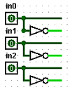
The figure below represents three inputs and their negations in an
easy-to-read standard layout. Use a similar layout in your circuit.
Show your canonical SOP and your working schematic to a lab instructor.
Task 4: Simplifying your schematic
Although the circuit that you designed above may implement the truth table, it may not be the most efficient implementation. Very often it is possible to simplify the logical expression representing a truth table using the rules of Boolean algebra rules. The procedure for doing this can be automated and represented graphically as a Karnaugh Map. Logisim implements a simplification procedure, and you can use it to reduce the size of your circuit.
Perform the following steps to apply the Karnaugh map optimization.
- Select main in the Explorer window and verify that the circuit representing the truth table is showing in Logisim’s circuit window. If not, select the project that contains the truth table circuit.
- Select Project from the menu bar and then select Analyze Circuit from the drop-down menu.
- In the Combinational Analysis window that appears
- Select the Minimized tab.
- Set the minimized logic expression as the working expression using the Set As Expression button. If Set As Expression cannot be selected, skip this step.
- Select the Build Circuit button to see the new implementation of the truth table.
- Say OK to building the circuit.
- Confirm replacement of your existing circuit.
- Admire your optimized circuit.
Also, take some time to investigate the other tabs on the Combinational Analysis window.
Show your simplified circuit to a lab instructor.
Task 5: Transistor implementation
Save the following Logisim circuit into your directory. Bet you pressed on the link and got a lot of XML. Logisim stores circuits in XML format, and, most likely, your browser just displayed the raw XML. You will have to do a right-click to save the circuit.
Once you have the circuit saved, open it in logisim. This should bring up a circuit with six independent subcircuits. You are going to experiment with each of these subcircuits to learn a little about how transistors are used to implement AND, OR, and NOT gates.
Pass 0 Pass 1
The N-type transistor, on the left, is closed, when its gate input is 0.
The P-type transistor, on the right, is closed, when its gate input is 0 and and is open when its gate input is 1.
Note that the P-type has the bubble on its gate. The indicates that it does the interesting thing when its control is 0.
Change the control input from 0 to 1 and back. Notice that often the output pin is floating, that is, connected to neither 0 or 1.
Real transistors aren’t quite like switches, but we won’t talk about that now.
Pulled inverters
By adding a pull resistor to your pass circuits, you can make a inverter. The pull resistor can be used to set a floating wire to a “default” value. We will use these in a later lab.
Try out your NMOS and PMOS inverters.
Many years ago, most computers were implemented with NMOS transistors. However, the NMOS inverter isn’t energy-efficient. When its input is 1, power is being dissipated by the pull register when has 1 on one end and 0 on the other. The only thing this lost power can do is heat up the circuit. That’s not good.
Inverters with N and P
The two transistor implementation eliminates the pull register. At any given time, one transistor is closed and the other is open. Modern processors are implemented with CMOS which allows both p-type and n-type transistors to be used on the chip.
Try out your two-transistor inverter.
Unfortunately, when the input to two-transistor inverter changes, there may be a very brief period when both transistors are closed. A great deal of current can be used during this time.
Pulled in Parallel
By placing two transistors in parallel in the lower half of the circuit, you can build a NOR (NOT-OR) gate.
Notice that an OR gate must be implemented as a NOT-NOR gate.
Pulled in Series
By placing two transistors in series in the lower half of the circuit, you can build a NAND (NOT-AND) gate.
And an AND gate must be implemented as a NOT-NAND.
CMOS gates
Here are examples of how NAND and NOR gates are implemented in CMOS.
In the CMOS implementation there are times when the wire connecting the two transistors in series is floating. Set both gates to have an internal floating wire.