In this lab you will experiment with flip-flips and other memory-like modules in Logisim.
The SR, JK, and D flip-flops in Logisim
We’re going to use Logisim to look at properties of common flip-flops illustrated in four Logisim contained in single circuit file that you should download to your computer.
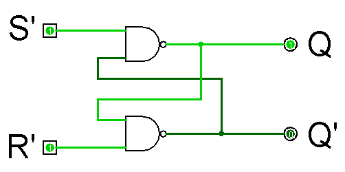
The SR flip-flop with NAND and NOR
First, play with the SR implemented with NAND gates
in the SR with NAND circuit.
Note that the inputs are labeled S’
and R’.
If Logisim supported overlining, these would be labeled
S
and R.
When an input variable is labeled by its inverse,
this means the input is negatively asserted;
that is, the interesting action occurs when the input is 0.
So to set Q to 1, you set S’
to 0; and to reset Q to 0, you set R’ to 0.
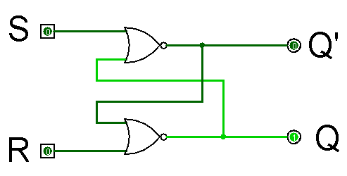
Next, try out the
SR with NOR circuit.
In this implementation
the inputs are positively asserted.
Notice that the Q output
isn’t where it used to be.
The D and JK flip-flops
Now, try the
JK and D flipflops circuit.
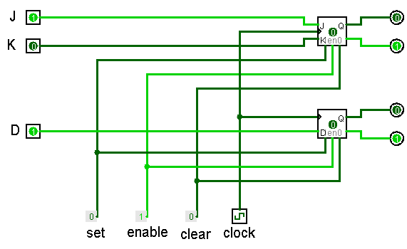
First, set D to 0 and click the clock twice. You should see that this changes the output of the D flip-flop. Set D back to 1.
There are four (22) different settings for the J and K flip-flops. Try each of these out a few times.
The other flip-flop inputs
Finally, it’s time to solve a puzzle with the
Flipflops triggering circuit.
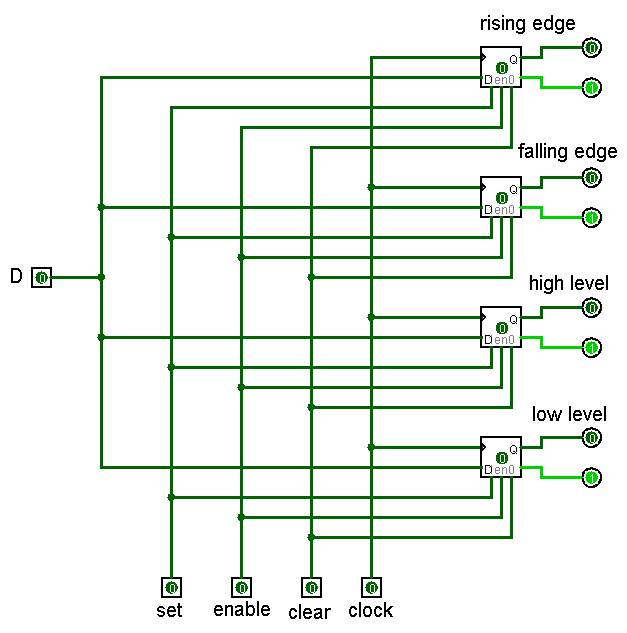
Note the set and clear (often called reset) inputs at the bottom of the circuit. These are asynchronous inputs. They change the output of a flip-flop independent of the clock. Exercise both of them, but leave them set to 0.
You can now click the clock many times, but nothing will happen until enable is set to 1.
With enable asserted, go through a few clock cycles while changing the D input. Notice when the four flip-flops actually change values in response to changes of the clock or D.
Using only the circuit inputs, get the four flip-flop circuits in a state where the two “edge” flip-flops are 1 and the two “level” flip-flops are 0.
This is a tricky little puzzle.
Alternative approaches to truth tables
You must remember how in the Introducing Logisim lab you implemented the following truth table with Logisim.
| inputs | output | ||
|---|---|---|---|
| a | b | c | x |
| 0 | 0 | 0 | 0 |
| 0 | 0 | 1 | 0 |
| 0 | 1 | 0 | 1 |
| 0 | 1 | 1 | 0 |
| 1 | 0 | 0 | 1 |
| 1 | 0 | 1 | 0 |
| 1 | 1 | 0 | 1 |
| 1 | 1 | 1 | 1 |
Reload your circuit. If you can’t find it, download a starter circuit and use Project ⇒ Analyze Circuit to build the circuit.
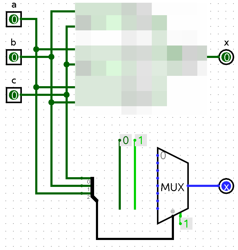
Using the multiplexer
Now let’s implement that circuit with a multiplexer. The Multiplexer is in the Plexers group. You want a mux with three select bits.
You’ll have to use the dreaded
Splitter to wire in the selector inputs.
Wire the three inputs, a, b and c,
into the single-bit ends of the splitter.
The whole circuit could look something like this before you connect
in the mux inputs.
Write up the mux implementation and that it agrees with the truth table on all eight possible input combinations.
The quickest way to test all eight is to use the Gray code sequence 000, 001, 011, 010, 110, 111, 101, 100.
Using the ROM
Next implement the circuit with a ROM from the Memory group. Think about how many address and data bits you need.
The part of the circuit with the ROM could look like this:
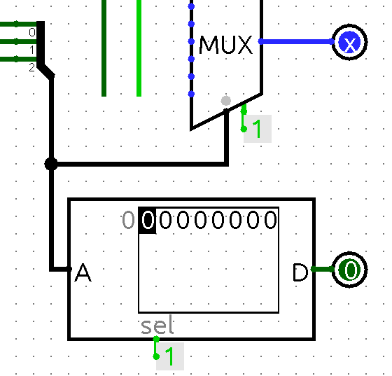
You will need to set the contents of the ROM to get your circuit to work.
Test your ROM implementation.
Animating with a clock counter
It’s tedious to go through all those eight combinations. Go to the Memory group and pick up a Counter. Set the counter up for 3 data bits. Also, go to Wiring group and bring back a Clock.
The counter has seven ports, but we are only going to use two of them.
The counter’s output will be connected to the bus carrying
the three inputs. Its clock input is connect to, of course, the clock.
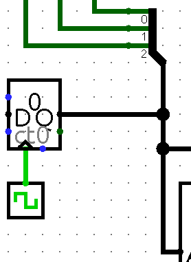
To avoid multiple drivers on the bus, you will need to change
a, b and c to be output pins.
You need to go to the simulate menu to get the clock to tick. Once it is going, it will go through all eight possible inputs every eight seconds.
Run the clock.