In this lab you will experiment with flip-flops using logisim and your breadboard.
Task 0 — Parts and partners
You will need the following equipment and components to create the circuits for today’s lab:
- your breadboard with the power supply constructed in the last lab
- 1 74HC112 dual J-K Flip-Flop
- 1 33 kΩ resistor network
Task 1 — The SR flip-flop with transistors
Starting with your breadboard you built in the
Building Logic Gates from Transistors lab,
build a SR flip-flop by connecting your two NOR gates
as shown below.

Practice setting the outputs of your flip-flop and then show the lab instructor how you can turn Q on and off by changing the inputs to R and S.
Task 2 — The SR, JK, and D flip-flops in logisim
We’re going to use logisim to look at properties of common flip-flops.
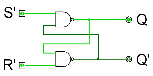
The SR flip-flop with NAND and NOR
Start by downloading and opening, in Logisim, a SR flip-flop implemented with NAND gates and a SR flip-flop implemented with NOR gates.
First, play with the SR implemented with NAND gates.
Note that the inputs are labeled S’
and R’.
If Logisim supported overlining, these would be labeled
S
and R.
When an input variable is labeled by its inverse,
this means the input is negatively asserted;
that is, the interesting action occurs when the input is 0.
So to set Q to 1, you set S’
to 0; and to reset Q to 0, you set R’ to 0.
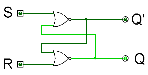
Next, play with the SR implemented with NOR gates.
In this implementation
the inputs are positively asserted.
Notice that the Q output
isn’t where it used to be.
The D and JK flip-flops
Now, download a
demonstration of D and JK flip-flops.
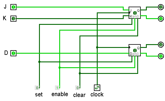
First, set D to 0 and click the clock twice. You should see that this changes the output of the D flip-flop. Set D back to 1.
There are four (22) different settings for the J and K flip-flops. Try each of these out a few times.
The other flip-flop inputs
Run Logisim on a
circuit with four different D flip-flops.
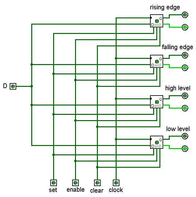
Note the set and clear (often called reset) inputs at the bottom of the circuit. These are asynchronous inputs. They change the output of a flip-flop independent of the clock. Exercise both of them, but leave them set to 0.
You can now click the clock many times, but nothing will happen until enable is set to 1.
With enable asserted, go through a few clock cycles while changing the D input. Notice when the four flip-flops actually change values in response to changes of the clock or D.
Describe, to your instructor, something interesting your learned during your time with Logisim. If you can’t think of anything else; using only the inputs, get the four flip-flop circuits in a state where the two “edge” flip-flops are 1 and the two “level” flip-flops are 0.
Task 3 — Cleaning up a bit
Before preceding to the next part of the lab, you need to remove everything from your breadboard except for the power supply circuits and the two LED switch circuits. In particular, remove your four NOT gates.
Return the four transistors, four 1 kΩ resistors, and four 10 kΩ resistors to your instructor.
Task 4 — The JK flip-flop with a 74112
The 7400 series
The 7400 series was the first significant family of integrated circuits. The family members are SSI (small scale integration) or MSI (medium scale integration) circuits that generally consist of about 100 transistors and implemented a small number of gates.
The chips were documented in The TTL Data Book for Design Engineers, first published by Texas Instruments in 1973. Most electrical engineers and many physicists cherished their copy of this book and fondly remember its bright orange cover. Several even knew the chip numbers from memory.
The 7400, which contained four two-input NAND gates, was the first
of the series.
The 7400 was packaged in a 14-pin
DIP (dual in-line package).
The pins of the chips were numbered counter-clockwise, with the pin 1
being immediately to the left of a notch on one end of the chip.
Power was always connected to the last pin, the one to the right of the
notch, and ground to the pin on the opposite corner from power.
Diagrams would specify the function of pins.
For example, on the 7400, one NAND gate had input
connections on pins 9
and 10 and an output connection on pin 8.

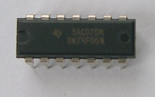
Wiring the 74112
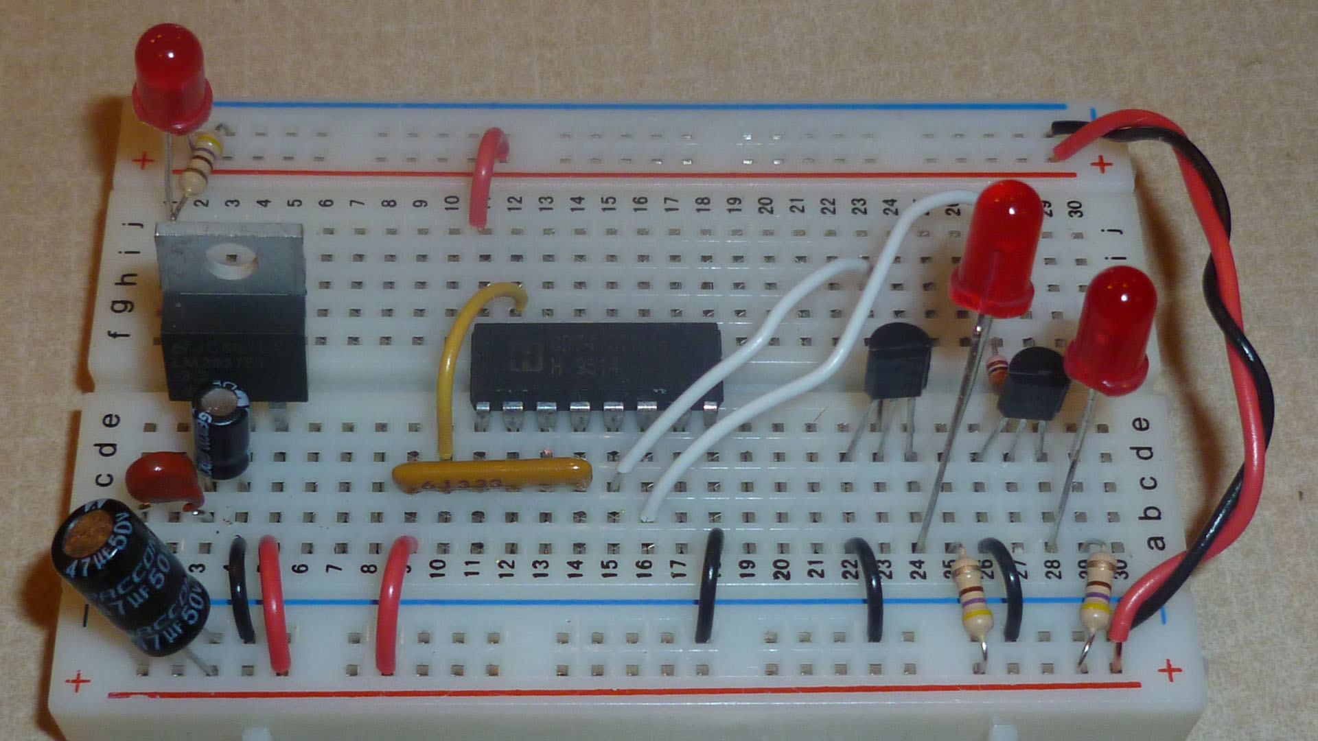
The 74112 (pronounced 74-112) contains two J-K Flip-Flop. Study the 74HC112E data sheet to discover the pin assignments for this chip. In this lab we are going to use F/F 1, the top flip-flop shown in the diagram on page 2 of the datasheet.
Start by disconnecting power from your breadboard. Integrated circuits are much more sensitive than discrete transistors. Even the capacitance on your hands could damage a chip.
Next plac your chip onto the breadboard and connecting it to ground and power. Then connect the two outputs of flip-flop 1 to the two LED switches.
In the previous lab we set a circuit’s input by moving a wire between ground and power. When this is done, there is a brief period when the input wire is connected to neither ground or power. That’s acceptable for a transistor like the 2N3904 but not for an integrated circuit.
To prevent these temporary disconnects, we are going to use the simple
pull-up resistor as illustrated in the figure below.
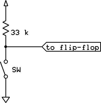
When the switch is open, the output (which is being routed to
the flip-flop) is connected the VDD through
a 33 kΩ resistor.
(You’ll see why 33 kΩ is chosen in a little while.)
When the switch is closed, the output is connected to ground.
You can continue to close the switch by moving a wire, just as you did
in previous labs, and the flip-flop input will continue to be connected.
However, do avoid touching the wire. You are just too charged up for that.
As you discovered by reading the datasheet, the J-K flip-flop has
five inputs:
R,
S,
J,
K,
and CP.
Because it would be tedious to connect five resistors in such
tight quarters, we are going to use a very small
SIP
(single in-line package) bussed resistor network which
contains five resistors
as shown in the following drawing:
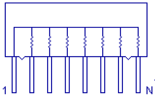
Pin 1 of the network will be connected to
VDD and the remaining pins will be connected
to inputs of the J-K flip-flop.
This allows you to build five pull-up resistors with one SIP and a connection
to VDD.
There is one more complication: The five inputs to the flip-flop are not
in adjacent rows. One is assigned to pin 15 and the other four to
pin 1 through pin 4.
The easiest way to solve this problem by running a wire
between pin 2 of the resistor network to pin 15 of the chip.
This is shown in the following picture.
Before you insert the resistor network into your circuit, take a careful look at the SIP. One of the pins is marked with a small dot. This the the common terminal shared by all five resistors. The package also is stamped with a number ending with the three digits 333. In the encoding of SMD (surface-mounted device) resistors, 333 encodes 33×103 or 33000.
Open a spreadsheet in OpenDocument Spreadsheet format and fill in the blanks. Show the instructor your completed spreadsheet.