In this lab you will make a few logic gates with transistors.
Task 0 — Parts and partners
You will need the following equipment and components to create the circuits for today’s lab:
- your breadboard with the power supply constructed in the last lab
- 1 multimeter
- 2 alligator clip leads for use with multimeter
- 6 1 kΩ resistors (Brown-Black-Red)
- 6 10 kΩ resistors (Brown-Black-Orange)
- 2 LED’s
- 6 NPN (2N3904) transistors
Task 1 — PNP & NPN
We can perform many control functions by connecting switches,
or transistors, in series or parallel.
In the example on the left below, we are using two
NPN transistors in parallel to connect the output to ground, or pass 0.
if either X or Y is one.
The circuit on the right uses two PNP transistors in series to
pass 1, if both X and Y
are zero.
Note that, when both circuits are receiving the same two inputs, exactly one will
be passing a value.
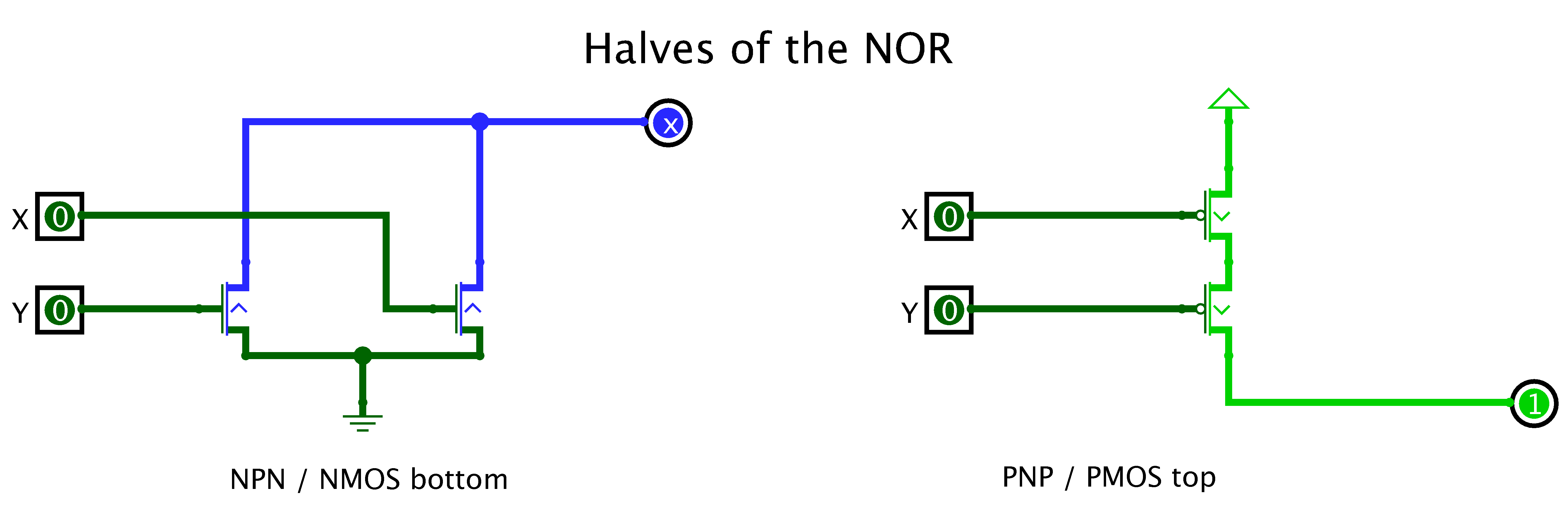
Go ahead and start up logisim on a downloaded copy of this transistor network. First, try out the two halves. Then join the halves together to form a real NOR that produces the right output for all four input combinations. You’ll have to remove some redundant input and output pins to make this work.
Now make a NAND. Start with another downloaded
logisim circuit.
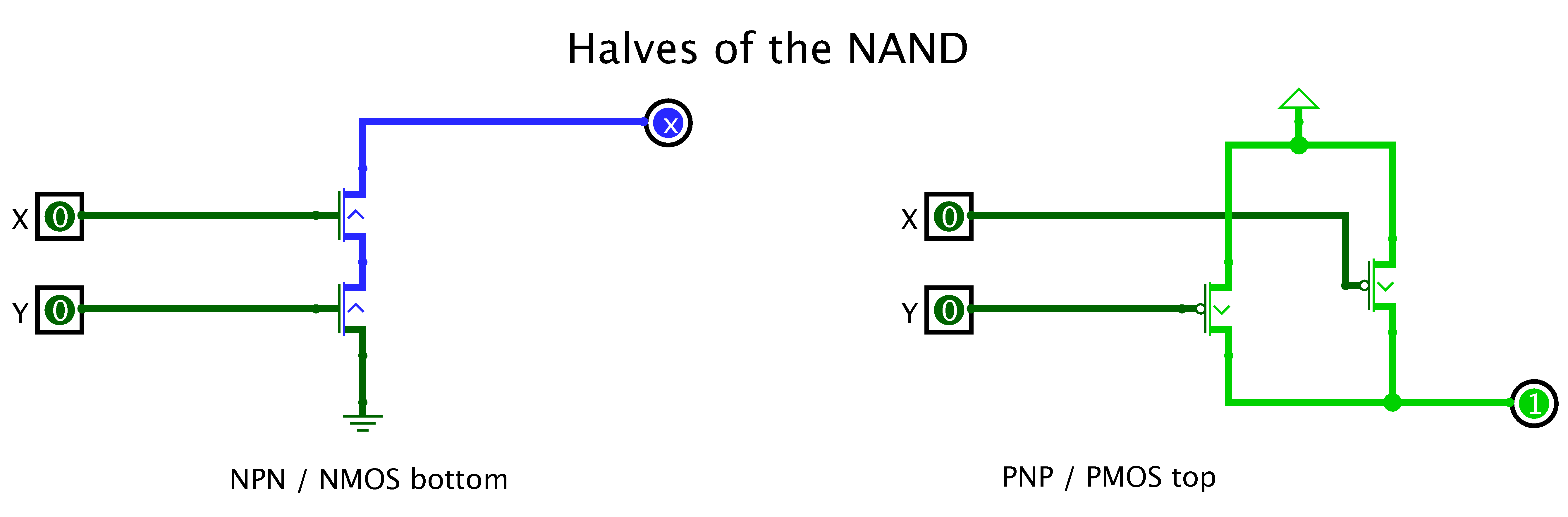
While the above examples were two-input series and parallel networks, we can extend these circuits to handle an arbitrary number of inputs. The PNP (top) and NPN (bottom) transistor networks must be designed so that there is no input combination in which both networks pass a value at the same time. If one network were passing 1 and the other were passing 0, we would have a short-circuit.
There are additional and more esoteric properties of transistors that restrict how they can pass values. This approach to implementing logic functions with transistors only works for inverting logic functions. In an inverting logic function, changing any input line from 0 to 1 will never change the output line from 0 to 1. This means that a non-inverting logic gate, such as the AND, must be built with two inverting logic gates, such as NAND followed by NOT.
Show your NOR and NAND implementations to a lab instructor.
Task 2 — NPN only
Today, integrated circuits are implemented in some form of CMOS (complementary metal-on-silicon). A few decades before that, RTL (resistor-transistor logic) and then TTL (transistor-transistor logic) were used. Before CMOS and TTL, there was a period where NMOS (N-type MOS) was used [One of the lab instructors even designed part of a chip that was implemented in NMOS in the dark ages.]
In NMOS, the PNP network is replaced by a single pull-up resistor.
When the NPN network doesn’t pass a 0, the output is “pulled-up” to 1.
Here’s a pull-up implementation of a NOR gate.
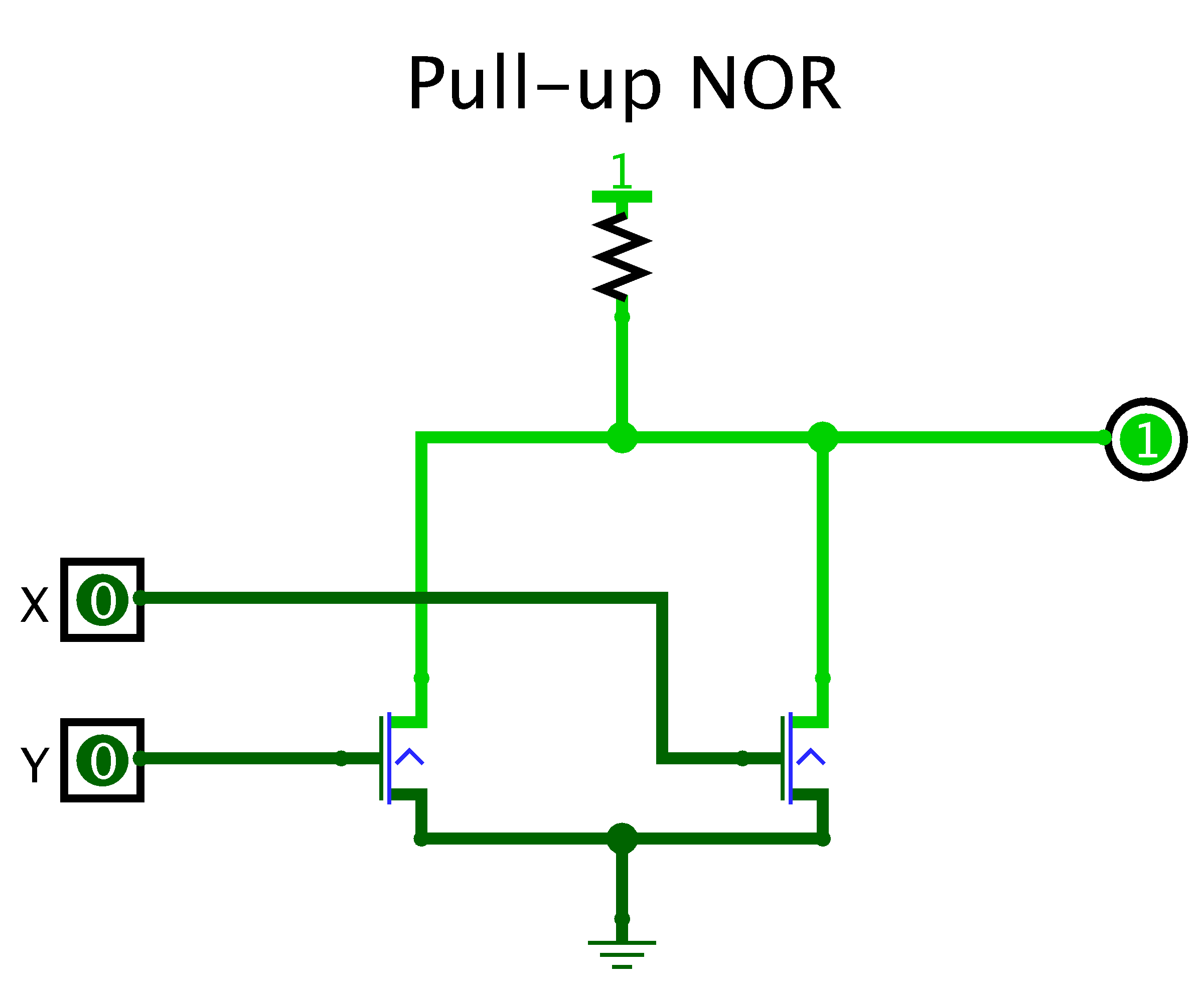
So why would anyone use two-transistor CMOS rather than one-transistor NMOS? There are several reasons. First, today’s computers are implemented with integrated circuits. The area required for a resistor on a chip is much larger than that required for a transistor. Second, because the 1 must be “pulled” through a resistor, it requires some time to charge up the output line when the output changes from 0 to 1. (Think of filling a swimming pool with a garden hose.) In CMOS, this is almost instantaneous. Third, when the 1 is being generated by the pull-up, it requires constant power and, consequently, produces heat. (Think of leaving the water running all the time.) In CMOS, power is not used when the circuit is in a stable state. The CMOS FET (field-effect transistor) is very similar to a switch. It is either off or on.
Modify your NOR and NAND implementations to use pull-ups.
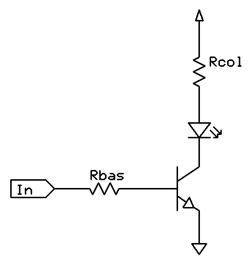
Task 3 — Building an inverter
The simplest circuit
is the inverter. Here is how the NOT gate can be implemented with MOSFET transistors.

When inverters are built with different
logic families,
they have radically different implementations.
For example, here is one way to realize an inverter in
the TTL (transistor-transistor logic) family.

An RTL (resistor-transistor logic)
inverter can be implemented with a couple of resistors and
a single transistor as shown below.
The input to the inverter is connected to
the transistor though a base resistor, Rbas.
There is a collector resistor, Rcol, that connects the high
voltage to the collector of the transistors.
We will use a 1 KΩ resistor for Rcol
and a 10 KΩ resistor for Rbas.
There’s nothing magic about these choices. We just happen to have a lot
of them.
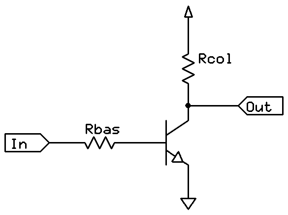
In the drawing above the triangle at the top is a connection to
VDD and the triangle at the bottom
is a connection to ground.
In the first part of the lab we are going to ask you to build four NOT gates and two LED switches. You need the switches because it would be very tedious to test your circuit with a multimeter.
We suggest that on one end of your breadboard, you create
the two LED switches.
Each is a single-input circuit that lights
up an LED when the circuit’s input is 1.
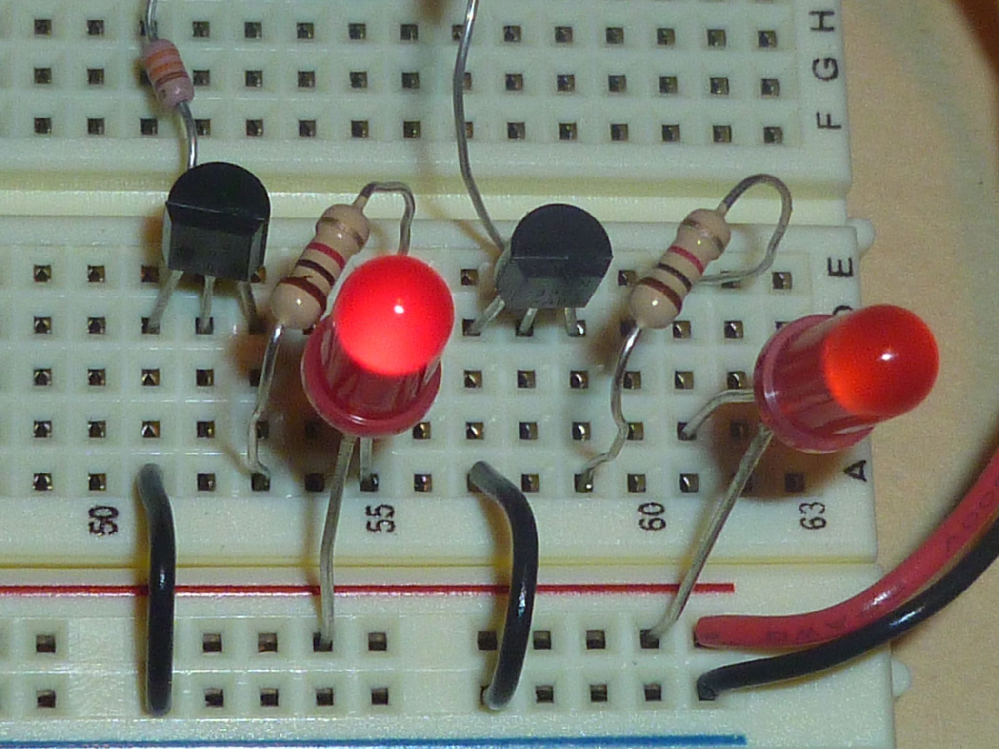
Because the NOT and the LED switch circuits are very similar, you should build and test the LED switches first.
Place the four NOT’s in the middle of the breadboard. We recommend that you put the NPN transistor and the collector resistor on the bottom half of your breadboard and use the base resistor to bridge between the top and bottom halves of the baseboard.
Show your LED switches and NOT circuits to your instructor after you have tested them.
Task 4 — A NOR Gate
In CMOS Boolean functions are generally implemented with NAND gates. Unfortunately, it is difficult to build a reliable NAND gate having more than two inputs with RTL. So, we are going to build a NOR. This is not a significant problem when building larger circuits. Any Boolean function can be implemented with two levels of NOR gates using a product of sums, similar to how a sum of products can be used in a two-level NAND implementation.
Here’s an RTL circuit for a two-input NOR.
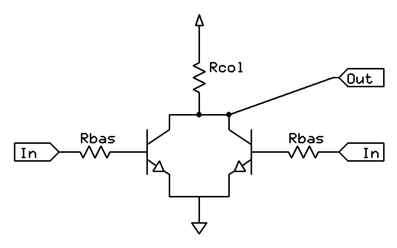
If you are thinking that an NOR looks like
two NOTs sharing a single pull-up transistor Rcol,
you are on the right track.
+
~=
But it’s even better than that because two
1K Ω resistors in parallel make a
500 Ω resistor and a
500 Ω resistor is good enough for our NOR.
(This means you don’t even have to remove the extra
1K Ω resistor to build your NOR.)
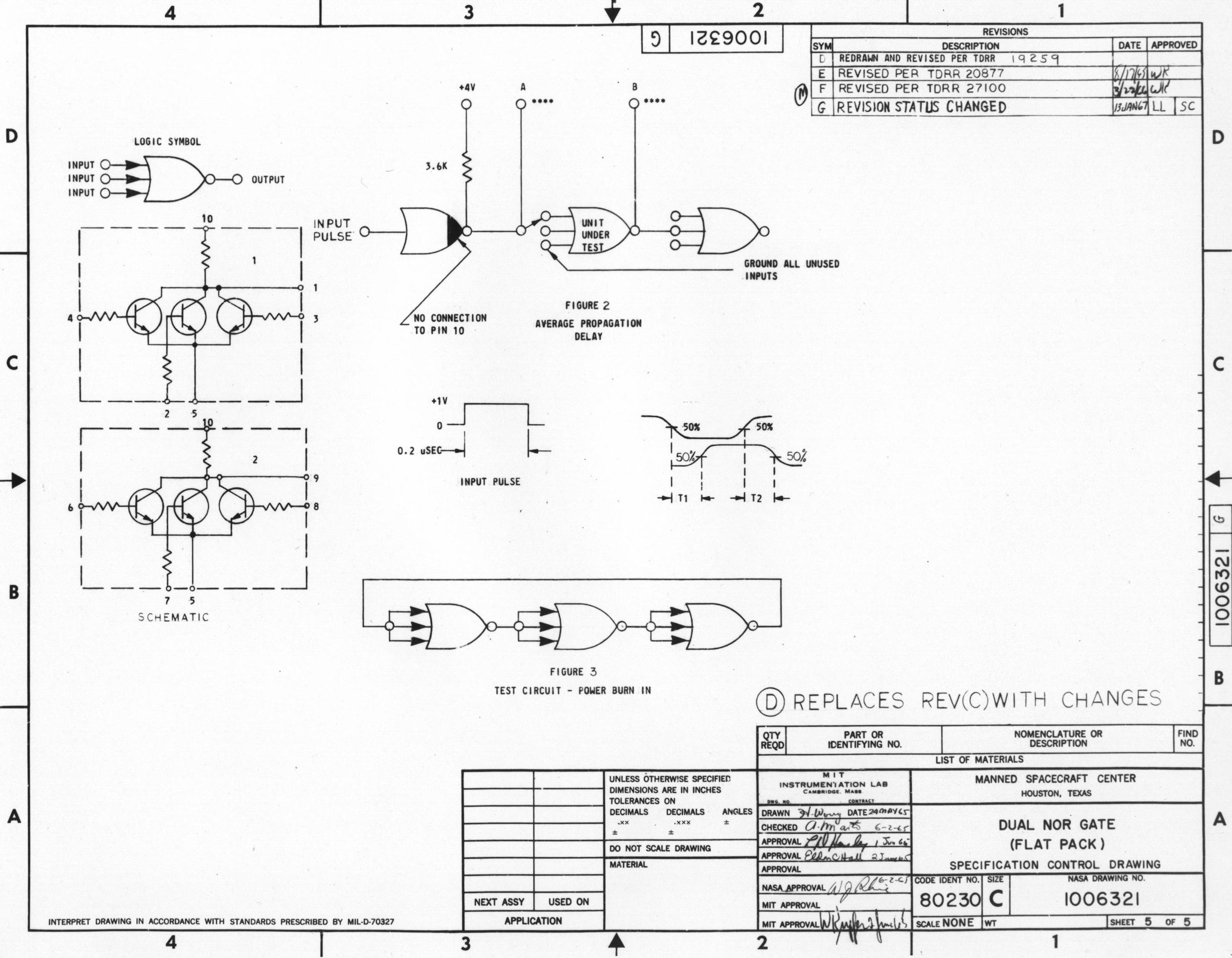
By the way, the Apollo Guidance Computer used about 2,800 RTL chips, each
containing two three-input NOR gates, for all the manned flights
to the moon.
If you click the image below, you will see that our NOR
differs little from NASA’s.
Now create your own version of this 1965 classic with a single NOR from two NOT’s by adding one wire!
Demonstrate the functionality of your NOR gate for your instructor.
Task 5 — An OR Gate
So, now you have one NOR and two NOT’s. Take advantage of the following Boolean identity to build an OR gate.
- x OR y = NOT(x NOR y)
Demonstrate the functionality of your OR gate for your instructor.
Task 6 — An AND Gate
Next use De Morgan’s law to build an AND gate.
- x AND y = (NOT x) NOR (NOT y)
Demonstrate the functionality of your AND gate for your instructor.
Preview of coming events: The SR flip-flop
Don’t tear up your breadboard.
Next week, you’ll build a SR flip-flop from two NOR
gates.
